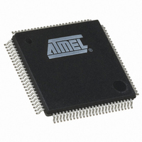
ATSAM3S4CA-AU Atmel, ATSAM3S4CA-AU Datasheet - Page 365

ATSAM3S4CA-AU
Manufacturer Part Number
ATSAM3S4CA-AU
Description
IC MCU 32BIT 256KB FLASH 100LQFP
Manufacturer
Atmel
Series
SAM3Sr
Specifications of ATSAM3S4CA-AU
Core Processor
ARM® Cortex-M3™
Core Size
32-Bit
Speed
64MHz
Connectivity
EBI/EMI, I²C, MMC, SPI, SSC, UART/USART, USB
Peripherals
Brown-out Detect/Reset, DMA, I²S, POR, PWM, WDT
Number Of I /o
79
Program Memory Size
256KB (256K x 8)
Program Memory Type
FLASH
Ram Size
48K x 8
Voltage - Supply (vcc/vdd)
1.62 V ~ 1.95 V
Data Converters
A/D 16x10/12b, D/A 2x12b
Oscillator Type
Internal
Operating Temperature
-40°C ~ 85°C
Package / Case
100-LQFP
Controller Family/series
ATSAM3S
No. Of I/o's
79
Ram Memory Size
48KB
Cpu Speed
64MHz
No. Of Timers
6
Rohs Compliant
Yes
Processor Series
ATSAM3x
Core
ARM Cortex M3
3rd Party Development Tools
JTRACE-CM3, MDK-ARM, RL-ARM, ULINK2
Development Tools By Supplier
ATSAM3S-EK
Cpu Family
AT91
Device Core
ARM Cortex-M3
Device Core Size
32b
Frequency (max)
64MHz
Total Internal Ram Size
48KB
# I/os (max)
79
Number Of Timers - General Purpose
6
Operating Supply Voltage (typ)
1.8/3.3V
Operating Supply Voltage (max)
1.95/3.6V
Operating Supply Voltage (min)
1.62V
On-chip Adc
16-chx12-bit
On-chip Dac
2-chx12-bit
Instruction Set Architecture
RISC
Operating Temp Range
-40C to 85C
Operating Temperature Classification
Industrial
Mounting
Surface Mount
Pin Count
100
Package Type
LQFP
Lead Free Status / RoHS Status
Lead free / RoHS Compliant
Eeprom Size
-
Lead Free Status / Rohs Status
Details
Available stocks
Company
Part Number
Manufacturer
Quantity
Price
Part Number:
ATSAM3S4CA-AU
Manufacturer:
ATMEL/爱特梅尔
Quantity:
20 000
- Current page: 365 of 1118
- Download datasheet (24Mb)
Figure 23-4. Standard and “CE don’t care” NAND Flash Application Examples
6500C–ATARM–8-Feb-11
SMC
PIO
PIO
D[7:0]
A[22:21]
NANDOE
NANDWE
NCSx
The address latch enable and command latch enable signals on the NAND Flash device are
driven by address bits A22 and A21of the address bus. Any bit of the address bus can also be
used for this purpose. The command, address or data words on the data bus of the NAND Flash
d e v i c e u s e th e i r o w n a d dr e s s e s w i th i n t h e N C S x a d d r es s s p a c e (c o n fi gu r e d b y
CCFG_SMCNFCS Register on the Bus Matrix User Interface). The chip enable (CE) signal of
the device and the ready/busy (R/B) signals are connected to PIO lines. The CE signal then
remains asserted even when NCS3 is not selected, preventing the device from returning to
standby mode. The NANDCS output signal should be used in accordance with the external
NAND Flash device type.
Two types of CE behavior exist depending on the NAND flash device:
Figure 23-4
Not Connected
• PIO Input with pull-up enabled (default state after reset)
• PIO Output set at level 1
• Standard NAND Flash devices require that the CE pin remains asserted Low continuously
• This restriction has been removed for “CE don’t care” NAND Flash devices. The NCSx signal
during the read busy period to prevent the device from returning to standby mode. Since the
SAM3S Static Memory Controller (SMC) asserts the NCSx signal High, it is necessary to
connect the CE pin of the NAND Flash device to a GPIO line, in order to hold it low during the
busy period preceding data read out.
can be directly connected to the CE pin of the NAND Flash device.
illustrates both topologies: Standard and “CE don’t care” NAND Flash.
CE
R/B
ALE
CLE
NOE
NWE
AD[7:0]
NAND Flash
SMC
PIO
D[7:0]
A[22:21]
NANDOE
NANDWE
NCSx
SAM3S Preliminary
CE
“CE don’t care”
NAND Flash
R/B
ALE
CLE
NOE
NWE
AD[7:0]
365
Related parts for ATSAM3S4CA-AU
Image
Part Number
Description
Manufacturer
Datasheet
Request
R

Part Number:
Description:
KIT EVAL FOR ATSAM3S4C
Manufacturer:
Atmel
Datasheet:

Part Number:
Description:
Development Boards & Kits - ARM EVAL KIT SAM3S8 & SAM3SD8 series
Manufacturer:
Atmel
Datasheet:

Part Number:
Description:
AT91 ARM Cortex M3-based Processor
Manufacturer:
ATMEL [ATMEL Corporation]
Datasheet:

Part Number:
Description:
DEV KIT FOR AVR/AVR32
Manufacturer:
Atmel
Datasheet:

Part Number:
Description:
INTERVAL AND WIPE/WASH WIPER CONTROL IC WITH DELAY
Manufacturer:
ATMEL Corporation
Datasheet:

Part Number:
Description:
Low-Voltage Voice-Switched IC for Hands-Free Operation
Manufacturer:
ATMEL Corporation
Datasheet:

Part Number:
Description:
MONOLITHIC INTEGRATED FEATUREPHONE CIRCUIT
Manufacturer:
ATMEL Corporation
Datasheet:

Part Number:
Description:
AM-FM Receiver IC U4255BM-M
Manufacturer:
ATMEL Corporation
Datasheet:

Part Number:
Description:
Monolithic Integrated Feature Phone Circuit
Manufacturer:
ATMEL Corporation
Datasheet:

Part Number:
Description:
Multistandard Video-IF and Quasi Parallel Sound Processing
Manufacturer:
ATMEL Corporation
Datasheet:

Part Number:
Description:
High-performance EE PLD
Manufacturer:
ATMEL Corporation
Datasheet:

Part Number:
Description:
8-bit Flash Microcontroller
Manufacturer:
ATMEL Corporation
Datasheet:


