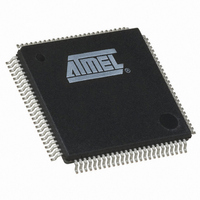
ATSAM3S4CA-AU Atmel, ATSAM3S4CA-AU Datasheet - Page 377

ATSAM3S4CA-AU
Manufacturer Part Number
ATSAM3S4CA-AU
Description
IC MCU 32BIT 256KB FLASH 100LQFP
Manufacturer
Atmel
Series
SAM3Sr
Specifications of ATSAM3S4CA-AU
Core Processor
ARM® Cortex-M3™
Core Size
32-Bit
Speed
64MHz
Connectivity
EBI/EMI, I²C, MMC, SPI, SSC, UART/USART, USB
Peripherals
Brown-out Detect/Reset, DMA, I²S, POR, PWM, WDT
Number Of I /o
79
Program Memory Size
256KB (256K x 8)
Program Memory Type
FLASH
Ram Size
48K x 8
Voltage - Supply (vcc/vdd)
1.62 V ~ 1.95 V
Data Converters
A/D 16x10/12b, D/A 2x12b
Oscillator Type
Internal
Operating Temperature
-40°C ~ 85°C
Package / Case
100-LQFP
Controller Family/series
ATSAM3S
No. Of I/o's
79
Ram Memory Size
48KB
Cpu Speed
64MHz
No. Of Timers
6
Rohs Compliant
Yes
Processor Series
ATSAM3x
Core
ARM Cortex M3
3rd Party Development Tools
JTRACE-CM3, MDK-ARM, RL-ARM, ULINK2
Development Tools By Supplier
ATSAM3S-EK
Cpu Family
AT91
Device Core
ARM Cortex-M3
Device Core Size
32b
Frequency (max)
64MHz
Total Internal Ram Size
48KB
# I/os (max)
79
Number Of Timers - General Purpose
6
Operating Supply Voltage (typ)
1.8/3.3V
Operating Supply Voltage (max)
1.95/3.6V
Operating Supply Voltage (min)
1.62V
On-chip Adc
16-chx12-bit
On-chip Dac
2-chx12-bit
Instruction Set Architecture
RISC
Operating Temp Range
-40C to 85C
Operating Temperature Classification
Industrial
Mounting
Surface Mount
Pin Count
100
Package Type
LQFP
Lead Free Status / RoHS Status
Lead free / RoHS Compliant
Eeprom Size
-
Lead Free Status / Rohs Status
Details
Available stocks
Company
Part Number
Manufacturer
Quantity
Price
Part Number:
ATSAM3S4CA-AU
Manufacturer:
ATMEL/爱特梅尔
Quantity:
20 000
- Current page: 377 of 1118
- Download datasheet (24Mb)
23.10 Automatic Wait States
23.10.1
Figure 23-13. Chip Select Wait State between a Read Access on NCS0 and a Write Access on NCS2
23.10.2
6500C–ATARM–8-Feb-11
Chip Select Wait States
Early Read Wait State
A[23:0]
D[7:0]
NCS0
NCS2
NWE
MCK
NRD
When multiple chip selects are handled, it is possible to configure the scrambling function per
chip select using the OCMS field in the SMC_OCMS registers.
Under certain circumstances, the SMC automatically inserts idle cycles between accesses to
avoid bus contention or operation conflict.
The SMC always inserts an idle cycle between 2 transfers on separate chip selects. This idle
cycle ensures that there is no bus contention between the de-activation of one device and the
activation of the next one.
During chip select wait state, all control lines are turned inactive: NWR, NCS[0..3], NRD lines are
all set to 1.
Figure 23-13
Select 2.
In some cases, the SMC inserts a wait state cycle between a write access and a read access to
allow time for the write cycle to end before the subsequent read cycle begins. This wait state is
not generated in addition to a chip select wait state. The early read cycle thus only occurs
between a write and read access to the same memory device (same chip select).
An early read wait state is automatically inserted if at least one of the following conditions is
valid:
illustrates a chip select wait state between access on Chip Select 0 and Chip
NRD_CYCLE
Read to Write
Wait State
Chip Select
Wait State
SAM3S Preliminary
NWE_CYCLE
377
Related parts for ATSAM3S4CA-AU
Image
Part Number
Description
Manufacturer
Datasheet
Request
R

Part Number:
Description:
KIT EVAL FOR ATSAM3S4C
Manufacturer:
Atmel
Datasheet:

Part Number:
Description:
Development Boards & Kits - ARM EVAL KIT SAM3S8 & SAM3SD8 series
Manufacturer:
Atmel
Datasheet:

Part Number:
Description:
AT91 ARM Cortex M3-based Processor
Manufacturer:
ATMEL [ATMEL Corporation]
Datasheet:

Part Number:
Description:
DEV KIT FOR AVR/AVR32
Manufacturer:
Atmel
Datasheet:

Part Number:
Description:
INTERVAL AND WIPE/WASH WIPER CONTROL IC WITH DELAY
Manufacturer:
ATMEL Corporation
Datasheet:

Part Number:
Description:
Low-Voltage Voice-Switched IC for Hands-Free Operation
Manufacturer:
ATMEL Corporation
Datasheet:

Part Number:
Description:
MONOLITHIC INTEGRATED FEATUREPHONE CIRCUIT
Manufacturer:
ATMEL Corporation
Datasheet:

Part Number:
Description:
AM-FM Receiver IC U4255BM-M
Manufacturer:
ATMEL Corporation
Datasheet:

Part Number:
Description:
Monolithic Integrated Feature Phone Circuit
Manufacturer:
ATMEL Corporation
Datasheet:

Part Number:
Description:
Multistandard Video-IF and Quasi Parallel Sound Processing
Manufacturer:
ATMEL Corporation
Datasheet:

Part Number:
Description:
High-performance EE PLD
Manufacturer:
ATMEL Corporation
Datasheet:

Part Number:
Description:
8-bit Flash Microcontroller
Manufacturer:
ATMEL Corporation
Datasheet:


