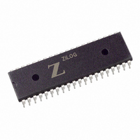
Z85C3008PSG Zilog, Z85C3008PSG Datasheet - Page 82

Z85C3008PSG
Manufacturer Part Number
Z85C3008PSG
Description
IC 8MHZ Z8500 CMOS SCC 40-DIP
Manufacturer
Zilog
Series
SCCr
Specifications of Z85C3008PSG
Processor Type
Z80
Features
Error Detection and Multiprotocol Support
Speed
8MHz
Voltage
5V
Mounting Type
Through Hole
Package / Case
40-DIP (0.620", 15.75mm)
Maximum Operating Temperature
+ 70 C
Minimum Operating Temperature
0 C
Mounting Style
Through Hole
Cpu Speed
8MHz
Digital Ic Case Style
DIP
No. Of Pins
40
Supply Voltage Range
5V
Operating Temperature Range
0°C To +70°C
Svhc
No SVHC (18-Jun-2010)
Base Number
85
Rohs Compliant
Yes
Clock Frequency
8MHz
Lead Free Status / RoHS Status
Lead free / RoHS Compliant
Other names
269-3930
Q2456016A
Z85C3008PSG
Q2456016A
Z85C3008PSG
Available stocks
Company
Part Number
Manufacturer
Quantity
Price
Company:
Part Number:
Z85C3008PSG
Manufacturer:
ZILOG
Quantity:
6 100
Company:
Part Number:
Z85C3008PSG
Manufacturer:
Zilog
Quantity:
6
Company:
Part Number:
Z85C3008PSG
Manufacturer:
TOSHIBA
Quantity:
3 500
Part Number:
Z85C3008PSG
Manufacturer:
ZILOG
Quantity:
20 000
Company:
Part Number:
Z85C3008PSGSCC
Manufacturer:
ZILOG
Quantity:
2
- Current page: 82 of 317
- Download datasheet (4Mb)
UM010901-0601
receiver. That is, if Auto Enables is on and the /DCD pin is
High, the receiver is disabled; while the /DCD pin is low,
the receiver is enabled.
Received characters are assembled, checked for errors,
and moved to the receive data FIFO (eight bytes on ESCC,
three bytes on NMOS/CMOS). The user can program the
SCC to generate an interrupt to the CPU or to request a
data read from a DMA when data is received.
On the NMOS/CMOS version, it generates the Receive
Character Available interrupt and DMA Request on Re-
ceive (if enabled). The receive interrupt and DMA request
is generated when there is at least one character in the
FIFO. The Rx Character Available (RCA) bit is set if there
is at least one byte available.
The ESCC generates the receive character available inter-
rupt and DMA request on Receive (if enabled) and is de-
pendent on WR7' bit D3. If this bit is reset to 0 (this mode
is comparable to the NMOS/CMOS version), the receive
interrupt and DMA request is generated when there is at
least one character in the FIFO. If WR7' bit D3 is set to 1,
the receive interrupt and DMA request are generated
when there are four bytes available in the Receive FIFO.
The RCA bit in RR0 follows the state of WR7' D3. The RCA
bit is set if there is at least one byte available, regardless
of the status of WR7' bit D3.
This is the initialization sequence for the receiver in Asyn-
chronous mode. First, WR4 selects the mode, then WR3
and WR5 select the various options. At this point, the other
registers should be initialized as necessary. When all of
this is complete, the receiver may be enabled by setting bit
D0 of WR3 to 1.
See Section 2.4.7 “The Receive Interrupt” for more details
on receive interrupts.
4.2.3 Asynchronous Initialization
The initialization sequence for Asynchronous mode is
shown in Table 4-3. All of the SCC’s registers should be re-
initialized after a channel or hardware reset. Also, WR4
should be programmed first after a reset.
WR9
WR4
WR3
WR5
Note:
* Initializes transmitter and receiver simultaneously.
At this point, the other registers should be initialized ac-
cording to the hardware design such as clocking,
I/O mode, etc. When this is completed, the transmitter is
enabled by setting WR5 bit D3 to 1 and the receiver is en-
abled by setting WR3 bit D0 to 1.
Reg
Table 4-3. Initialization Sequence
Bit No Description
6, 7
3, 2
0, 1
6, 7
7, 6
6, 5
5
1
Asynchronous Mode
Hardware or channel Reset
Select Async Mode and the number
of stop bits*
Select parity*
Select clock mode*
Select number of receive bits per
character
Select Auto Enables Mode*
Select number of bits/char for
transmitter
Select modem control (RTS)
SCC™/ESCC™ User’s Manual
Data Communication Modes
4-7
4
Related parts for Z85C3008PSG
Image
Part Number
Description
Manufacturer
Datasheet
Request
R

Part Number:
Description:
Manufacturer:
Zilog, Inc.
Datasheet:

Part Number:
Description:
Cmos Scc Serial Communications Controller
Manufacturer:
ZiLOG Semiconductor
Datasheet:

Part Number:
Description:
Communication Controllers, ZILOG INTELLIGENT PERIPHERAL CONTROLLER (ZIP)
Manufacturer:
Zilog, Inc.
Datasheet:

Part Number:
Description:
KIT DEV FOR Z8 ENCORE 16K TO 64K
Manufacturer:
Zilog
Datasheet:

Part Number:
Description:
KIT DEV Z8 ENCORE XP 28-PIN
Manufacturer:
Zilog
Datasheet:

Part Number:
Description:
DEV KIT FOR Z8 ENCORE 8K/4K
Manufacturer:
Zilog
Datasheet:

Part Number:
Description:
KIT DEV Z8 ENCORE XP 28-PIN
Manufacturer:
Zilog
Datasheet:

Part Number:
Description:
DEV KIT FOR Z8 ENCORE 4K TO 8K
Manufacturer:
Zilog
Datasheet:

Part Number:
Description:
CMOS Z8 microcontroller. ROM 16 Kbytes, RAM 256 bytes, speed 16 MHz, 32 lines I/O, 3.0V to 5.5V
Manufacturer:
Zilog, Inc.
Datasheet:

Part Number:
Description:
Low-cost microcontroller. 512 bytes ROM, 61 bytes RAM, 8 MHz
Manufacturer:
Zilog, Inc.
Datasheet:

Part Number:
Description:
Z8 4K OTP Microcontroller
Manufacturer:
Zilog, Inc.
Datasheet:

Part Number:
Description:
CMOS SUPER8 ROMLESS MCU
Manufacturer:
Zilog, Inc.
Datasheet:

Part Number:
Description:
SL1866 CMOSZ8 OTP Microcontroller
Manufacturer:
Zilog, Inc.
Datasheet:


