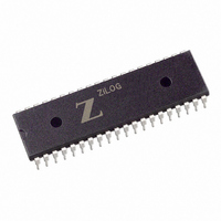
Z85C3008PSG Zilog, Z85C3008PSG Datasheet - Page 27

Z85C3008PSG
Manufacturer Part Number
Z85C3008PSG
Description
IC 8MHZ Z8500 CMOS SCC 40-DIP
Manufacturer
Zilog
Series
SCCr
Specifications of Z85C3008PSG
Processor Type
Z80
Features
Error Detection and Multiprotocol Support
Speed
8MHz
Voltage
5V
Mounting Type
Through Hole
Package / Case
40-DIP (0.620", 15.75mm)
Maximum Operating Temperature
+ 70 C
Minimum Operating Temperature
0 C
Mounting Style
Through Hole
Cpu Speed
8MHz
Digital Ic Case Style
DIP
No. Of Pins
40
Supply Voltage Range
5V
Operating Temperature Range
0°C To +70°C
Svhc
No SVHC (18-Jun-2010)
Base Number
85
Rohs Compliant
Yes
Clock Frequency
8MHz
Lead Free Status / RoHS Status
Lead free / RoHS Compliant
Other names
269-3930
Q2456016A
Z85C3008PSG
Q2456016A
Z85C3008PSG
Available stocks
Company
Part Number
Manufacturer
Quantity
Price
Company:
Part Number:
Z85C3008PSG
Manufacturer:
ZILOG
Quantity:
6 100
Company:
Part Number:
Z85C3008PSG
Manufacturer:
Zilog
Quantity:
6
Company:
Part Number:
Z85C3008PSG
Manufacturer:
TOSHIBA
Quantity:
3 500
Part Number:
Z85C3008PSG
Manufacturer:
ZILOG
Quantity:
20 000
Company:
Part Number:
Z85C3008PSGSCC
Manufacturer:
ZILOG
Quantity:
2
- Current page: 27 of 317
- Download datasheet (4Mb)
SCC™/ESCC™ User’s Manual
Interfacing the SCC/ESCC
2.2 Z80X30 INTERFACE TIMING (Continued)
2.2.5 Z80C30 Register Enhancement
The Z80C30 has an enhancement to the NMOS Z8030
register set, which is the addition of a 10x19 SDLC Frame
Status FIFO. When WR15 bit D2=1, the SDLC Frame Sta-
tus FIFO is enabled, and it changes the functionality of
RR6 and RR7. See Section 4.4.3 for more details on this
feature.
2.2.6 Z80230 Register Enhancements
In addition to the Z80C30 enhancements, the 80230 has
several enhancements to the SCC register set. These in-
clude the addition of Write Register 7 Prime (WR7'), and
the ability to read registers that are read only in the 8030.
Write Register 7' is addressed by setting WR15 bit, D0=1
and then addressing WR7. Figure 2-4 shows the register
bit location of the six features enabled through this
register. All writes to address seven are to WR7' when
WR15, D0=1. Refer to Chapter 5 for detailed information
on WR7'.
2-8
WR7'
D7 D6 D5 D4 D3 D2 D1 D0
Figure 2-4. Write Register 7 Prime (WR7')
Auto Tx Flag
Auto EOM Reset
Auto RTS Turnoff
Rx FIFO Half Full
DTR/REQ Timing M
Tx FIFO Empty
External Read Enab
0
WR7' bit D6=1, enables the extended read register capa-
bility. This allows the user to read the contents of WR3,
WR4, WR5, WR7' and WR10 by reading RR9, RR4, RR5,
RR14 and RR11, respectively. When WR7' D6=0, these
write registers are write only.
Table 2-3 shows what functions are enabled for the various
combinations of register bit enables. See Table 2-1 (Shift
Left) and Table 2-2 (Shift Right) for the register address map
with the SDLC FIFO enabled only and the map with both the
extended read and SDLC FIFO features enabled.
Bit D2 Bit D0 Bit D6 Functions Enabled
0
0
1
1
1
WR15
1
1
0
1
1
Table 2-3. Z80230 SDLC/HDLC
WR7'
Enhancement Options
X
0
1
0
1
WR7' enabled only
WR7' with extended read
enabled
10x19 SDLC FIFO
enhancement
enabled only
10x19 SDLC FIFO and WR7'
10x19 SDLC FIFO and WR7'
with extended read enabled
UM010901-0601
Related parts for Z85C3008PSG
Image
Part Number
Description
Manufacturer
Datasheet
Request
R

Part Number:
Description:
Manufacturer:
Zilog, Inc.
Datasheet:

Part Number:
Description:
Cmos Scc Serial Communications Controller
Manufacturer:
ZiLOG Semiconductor
Datasheet:

Part Number:
Description:
Communication Controllers, ZILOG INTELLIGENT PERIPHERAL CONTROLLER (ZIP)
Manufacturer:
Zilog, Inc.
Datasheet:

Part Number:
Description:
KIT DEV FOR Z8 ENCORE 16K TO 64K
Manufacturer:
Zilog
Datasheet:

Part Number:
Description:
KIT DEV Z8 ENCORE XP 28-PIN
Manufacturer:
Zilog
Datasheet:

Part Number:
Description:
DEV KIT FOR Z8 ENCORE 8K/4K
Manufacturer:
Zilog
Datasheet:

Part Number:
Description:
KIT DEV Z8 ENCORE XP 28-PIN
Manufacturer:
Zilog
Datasheet:

Part Number:
Description:
DEV KIT FOR Z8 ENCORE 4K TO 8K
Manufacturer:
Zilog
Datasheet:

Part Number:
Description:
CMOS Z8 microcontroller. ROM 16 Kbytes, RAM 256 bytes, speed 16 MHz, 32 lines I/O, 3.0V to 5.5V
Manufacturer:
Zilog, Inc.
Datasheet:

Part Number:
Description:
Low-cost microcontroller. 512 bytes ROM, 61 bytes RAM, 8 MHz
Manufacturer:
Zilog, Inc.
Datasheet:

Part Number:
Description:
Z8 4K OTP Microcontroller
Manufacturer:
Zilog, Inc.
Datasheet:

Part Number:
Description:
CMOS SUPER8 ROMLESS MCU
Manufacturer:
Zilog, Inc.
Datasheet:

Part Number:
Description:
SL1866 CMOSZ8 OTP Microcontroller
Manufacturer:
Zilog, Inc.
Datasheet:


