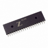
Z85C3008PSG Zilog, Z85C3008PSG Datasheet - Page 152

Z85C3008PSG
Manufacturer Part Number
Z85C3008PSG
Description
IC 8MHZ Z8500 CMOS SCC 40-DIP
Manufacturer
Zilog
Series
SCCr
Specifications of Z85C3008PSG
Processor Type
Z80
Features
Error Detection and Multiprotocol Support
Speed
8MHz
Voltage
5V
Mounting Type
Through Hole
Package / Case
40-DIP (0.620", 15.75mm)
Maximum Operating Temperature
+ 70 C
Minimum Operating Temperature
0 C
Mounting Style
Through Hole
Cpu Speed
8MHz
Digital Ic Case Style
DIP
No. Of Pins
40
Supply Voltage Range
5V
Operating Temperature Range
0°C To +70°C
Svhc
No SVHC (18-Jun-2010)
Base Number
85
Rohs Compliant
Yes
Clock Frequency
8MHz
Lead Free Status / RoHS Status
Lead free / RoHS Compliant
Other names
269-3930
Q2456016A
Z85C3008PSG
Q2456016A
Z85C3008PSG
Available stocks
Company
Part Number
Manufacturer
Quantity
Price
Company:
Part Number:
Z85C3008PSG
Manufacturer:
ZILOG
Quantity:
6 100
Company:
Part Number:
Z85C3008PSG
Manufacturer:
Zilog
Quantity:
6
Company:
Part Number:
Z85C3008PSG
Manufacturer:
TOSHIBA
Quantity:
3 500
Part Number:
Z85C3008PSG
Manufacturer:
ZILOG
Quantity:
20 000
Company:
Part Number:
Z85C3008PSGSCC
Manufacturer:
ZILOG
Quantity:
2
- Current page: 152 of 317
- Download datasheet (4Mb)
UM010901-0601
Z8500/Z8500A Peripherals
Figure 11 depicts logic that can be used in interfacing the
Z80H CPU to the Z8500/Z8500A peripherals. This logic is
the same as that shown in Figure 5, except that a
synchronizing flip-flop is used to recognize an Interrupt
Acknowledge cycle. Since Z8500 peripherals do not rely
upon PCLK except during Interrupt Acknowledge cycles,
synchronization need occur only at that time. Since the
CPU and the peripherals are running at different speeds,
/INTACK and /RD must be synchronized to the Z8500
peripherals clock.
During I/O and normal memory access cycles, the
synchronizing flip-flop and the Shift register remain
cleared because the /M1 signal is inactive. During opcode
fetch cycles, the flip-flop and the Shift register again
remain cleared, but this time because the /MREQ signal is
active. The synchronizing flip-flop allows an Interrupt
Acknowledge cycle to be recognized on the rising edge of
T2 when /M1 is active and /MREQ is inactive, generating
the INTA signal. When INTA is active, the Shift register can
clock and generate /INTACK to the peripheral and /WAIT
to the CPU. The Shift register delays the generation of
/READ to the peripheral until the daisy chain settles. The
Figure 10. Z80A/Z80B CPU to Z8500/Z8500A Peripheral Interrupt Acknowledge Interface Timing
/WAIT signal is removed when sufficient time has been
allowed for the interrupt vector data to be valid.
Figure 12 illustrates Interrupt Acknowledge cycle timing for
the Z80H CPU to Z8500 peripheral interface. Figure 13
illustrates Interrupt Acknowledge cycle timing for the Z80H
CPU to Z8500A peripheral interface. These timing result
from the logic in Figure 11. Should more Wait states be
required, the needed time should be calculated in terms of
PCLKs, not CPU clocks.
Z80 CPU to Z80 and Z8500 Peripherals
In a Z80 system, a combination of Z80 peripherals and
Z8500 peripherals can be used compatibly. While there is
no restriction on the placement of the Z8500 peripherals in
the daisy chain, it is recommended that they be placed
early in the chain to minimize propagation delays during
RET1 cycles.
During an Interrupt Acknowledge cycle, the IEO line from
Z8500 peripherals changes to reflect the interrupt status.
Time should be allowed for this change to ripple through
the remainder of the daisy chain before activating /IORQ
to the Z80 peripherals, or /READ to the Z8500 peripherals.
Interfacing Z80
®
CPUs to the Z8500 Peripheral Family
Application Note
6-17
6
Related parts for Z85C3008PSG
Image
Part Number
Description
Manufacturer
Datasheet
Request
R

Part Number:
Description:
Manufacturer:
Zilog, Inc.
Datasheet:

Part Number:
Description:
Cmos Scc Serial Communications Controller
Manufacturer:
ZiLOG Semiconductor
Datasheet:

Part Number:
Description:
Communication Controllers, ZILOG INTELLIGENT PERIPHERAL CONTROLLER (ZIP)
Manufacturer:
Zilog, Inc.
Datasheet:

Part Number:
Description:
KIT DEV FOR Z8 ENCORE 16K TO 64K
Manufacturer:
Zilog
Datasheet:

Part Number:
Description:
KIT DEV Z8 ENCORE XP 28-PIN
Manufacturer:
Zilog
Datasheet:

Part Number:
Description:
DEV KIT FOR Z8 ENCORE 8K/4K
Manufacturer:
Zilog
Datasheet:

Part Number:
Description:
KIT DEV Z8 ENCORE XP 28-PIN
Manufacturer:
Zilog
Datasheet:

Part Number:
Description:
DEV KIT FOR Z8 ENCORE 4K TO 8K
Manufacturer:
Zilog
Datasheet:

Part Number:
Description:
CMOS Z8 microcontroller. ROM 16 Kbytes, RAM 256 bytes, speed 16 MHz, 32 lines I/O, 3.0V to 5.5V
Manufacturer:
Zilog, Inc.
Datasheet:

Part Number:
Description:
Low-cost microcontroller. 512 bytes ROM, 61 bytes RAM, 8 MHz
Manufacturer:
Zilog, Inc.
Datasheet:

Part Number:
Description:
Z8 4K OTP Microcontroller
Manufacturer:
Zilog, Inc.
Datasheet:

Part Number:
Description:
CMOS SUPER8 ROMLESS MCU
Manufacturer:
Zilog, Inc.
Datasheet:

Part Number:
Description:
SL1866 CMOSZ8 OTP Microcontroller
Manufacturer:
Zilog, Inc.
Datasheet:


