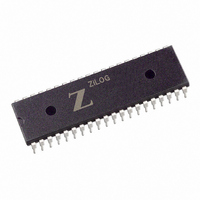
Z85C3008PSG Zilog, Z85C3008PSG Datasheet - Page 17

Z85C3008PSG
Manufacturer Part Number
Z85C3008PSG
Description
IC 8MHZ Z8500 CMOS SCC 40-DIP
Manufacturer
Zilog
Series
SCCr
Specifications of Z85C3008PSG
Processor Type
Z80
Features
Error Detection and Multiprotocol Support
Speed
8MHz
Voltage
5V
Mounting Type
Through Hole
Package / Case
40-DIP (0.620", 15.75mm)
Maximum Operating Temperature
+ 70 C
Minimum Operating Temperature
0 C
Mounting Style
Through Hole
Cpu Speed
8MHz
Digital Ic Case Style
DIP
No. Of Pins
40
Supply Voltage Range
5V
Operating Temperature Range
0°C To +70°C
Svhc
No SVHC (18-Jun-2010)
Base Number
85
Rohs Compliant
Yes
Clock Frequency
8MHz
Lead Free Status / RoHS Status
Lead free / RoHS Compliant
Other names
269-3930
Q2456016A
Z85C3008PSG
Q2456016A
Z85C3008PSG
Available stocks
Company
Part Number
Manufacturer
Quantity
Price
Company:
Part Number:
Z85C3008PSG
Manufacturer:
ZILOG
Quantity:
6 100
Company:
Part Number:
Z85C3008PSG
Manufacturer:
Zilog
Quantity:
6
Company:
Part Number:
Z85C3008PSG
Manufacturer:
TOSHIBA
Quantity:
3 500
Part Number:
Z85C3008PSG
Manufacturer:
ZILOG
Quantity:
20 000
Company:
Part Number:
Z85C3008PSGSCC
Manufacturer:
ZILOG
Quantity:
2
- Current page: 17 of 317
- Download datasheet (4Mb)
UM010901-0601
1.4.1 Pins Common to both Z85X30 and
Z80X30
/CTSA, /CTSB. Clear To Send (inputs, active Low). These
pins function as transmitter enables if they are pro-
grammed for Auto Enable (WR3, D5=1). A Low on the in-
puts enables the respective transmitters. If not pro-
grammed as Auto Enable, they may be used as general-
purpose inputs. Both inputs are Schmitt-trigger buffered to
accommodate slow rise-time inputs. The SCC detects
pulses on these inputs and can interrupt the CPU on both
logic level transitions.
/DCDA, /DCDB. Data Carrier Detect (inputs, active Low).
These pins function as receiver enables if they are pro-
grammed for Auto Enable (WR3, D5=1); otherwise, they
are used as general-purpose input pins. Both pins are
Schmitt-trigger buffered to accommodate slow rise time
signals. The SCC detects pulses on these pins and can in-
terrupt the CPU on both logic level transitions.
/RTSA, /RTSB. Request To Send (outputs, active Low).
The /RTS pins can be used as general-purpose outputs or
with the Auto Enable feature. When used with Auto Enable
ON (WR3, D5=1) in asynchronous mode, the /RTS pin
goes High after the transmitter is empty. When Auto En-
able is OFF, the /RTS pins are used as general-purpose
/DTR//REQA
Figure 1-6. Z80X30 DIP Pin Assignments
/W//REQA
/INTACK
/SYNCA
/RTxCA
/TRxCA
/DCDA
/RTSA
/CTSA
RxDA
TxDA
PCLK
VCC
AD1
AD3
AD5
AD7
/INT
IEO
IEI
1
2
3
4
5
6
7
8
9
10
11
12
13
14
15
16
17
18
19
20
Z80X30
40
39
38
37
36
35
34
33
32
31
30
29
28
27
26
25
24
23
22
21
AD0
AD2
AD4
AD6
/DS
/AS
R//W
/CS0
CS1
GND
/W//REQB
/SYNCB
/RTxCB
RxDB
/TRxCB
TxDB
/DTR//REQB
RTSB
/CTSB
/DCDB
outputs, and, they strictly follow the inverse state of WR5,
bit D1.
ESCC and 85C30:
In SDLC mode, the /RTS pins can be programmed to
be deasserted when the closing flag of the message
clears the TxD pin, if WR7' D2 is set .
/SYNCA, /SYNCB . Synchronization (inputs or outputs, ac-
tive Low). These pins can act either as inputs, outputs, or
part of the crystal oscillator circuit. In the Asynchronous
Receive mode (crystal oscillator option not selected),
these pins are inputs similar to CTS and DCD. In this
mode, transitions on these lines affect the state of the Syn-
chronous/Hunt status bits in Read Register 0 but have no
other function.
In External Synchronization mode, with the crystal oscilla-
tor not selected, these lines also act as inputs. In this
mode, /SYNC is driven Low to receive clock cycles after
the last bit in the synchronous character is received. Char-
acter assembly begins on the rising edge of the receive
clock immediately preceding the activation of SYNC.
In the Internal Synchronization mode (Monosync and Bi-
sync) with the crystal oscillator not selected, these pins
act as outputs and are active only during the part of the
Figure 1-7. Z80X30 PLCC Pin Assignments
SCC™/ESCC™ User’s Manual
General Description
1-7
1
Related parts for Z85C3008PSG
Image
Part Number
Description
Manufacturer
Datasheet
Request
R

Part Number:
Description:
Manufacturer:
Zilog, Inc.
Datasheet:

Part Number:
Description:
Cmos Scc Serial Communications Controller
Manufacturer:
ZiLOG Semiconductor
Datasheet:

Part Number:
Description:
Communication Controllers, ZILOG INTELLIGENT PERIPHERAL CONTROLLER (ZIP)
Manufacturer:
Zilog, Inc.
Datasheet:

Part Number:
Description:
KIT DEV FOR Z8 ENCORE 16K TO 64K
Manufacturer:
Zilog
Datasheet:

Part Number:
Description:
KIT DEV Z8 ENCORE XP 28-PIN
Manufacturer:
Zilog
Datasheet:

Part Number:
Description:
DEV KIT FOR Z8 ENCORE 8K/4K
Manufacturer:
Zilog
Datasheet:

Part Number:
Description:
KIT DEV Z8 ENCORE XP 28-PIN
Manufacturer:
Zilog
Datasheet:

Part Number:
Description:
DEV KIT FOR Z8 ENCORE 4K TO 8K
Manufacturer:
Zilog
Datasheet:

Part Number:
Description:
CMOS Z8 microcontroller. ROM 16 Kbytes, RAM 256 bytes, speed 16 MHz, 32 lines I/O, 3.0V to 5.5V
Manufacturer:
Zilog, Inc.
Datasheet:

Part Number:
Description:
Low-cost microcontroller. 512 bytes ROM, 61 bytes RAM, 8 MHz
Manufacturer:
Zilog, Inc.
Datasheet:

Part Number:
Description:
Z8 4K OTP Microcontroller
Manufacturer:
Zilog, Inc.
Datasheet:

Part Number:
Description:
CMOS SUPER8 ROMLESS MCU
Manufacturer:
Zilog, Inc.
Datasheet:

Part Number:
Description:
SL1866 CMOSZ8 OTP Microcontroller
Manufacturer:
Zilog, Inc.
Datasheet:


