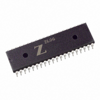
Z85C3008PSG Zilog, Z85C3008PSG Datasheet - Page 164

Z85C3008PSG
Manufacturer Part Number
Z85C3008PSG
Description
IC 8MHZ Z8500 CMOS SCC 40-DIP
Manufacturer
Zilog
Series
SCCr
Specifications of Z85C3008PSG
Processor Type
Z80
Features
Error Detection and Multiprotocol Support
Speed
8MHz
Voltage
5V
Mounting Type
Through Hole
Package / Case
40-DIP (0.620", 15.75mm)
Maximum Operating Temperature
+ 70 C
Minimum Operating Temperature
0 C
Mounting Style
Through Hole
Cpu Speed
8MHz
Digital Ic Case Style
DIP
No. Of Pins
40
Supply Voltage Range
5V
Operating Temperature Range
0°C To +70°C
Svhc
No SVHC (18-Jun-2010)
Base Number
85
Rohs Compliant
Yes
Clock Frequency
8MHz
Lead Free Status / RoHS Status
Lead free / RoHS Compliant
Other names
269-3930
Q2456016A
Z85C3008PSG
Q2456016A
Z85C3008PSG
Available stocks
Company
Part Number
Manufacturer
Quantity
Price
Company:
Part Number:
Z85C3008PSG
Manufacturer:
ZILOG
Quantity:
6 100
Company:
Part Number:
Z85C3008PSG
Manufacturer:
Zilog
Quantity:
6
Company:
Part Number:
Z85C3008PSG
Manufacturer:
TOSHIBA
Quantity:
3 500
Part Number:
Z85C3008PSG
Manufacturer:
ZILOG
Quantity:
20 000
Company:
Part Number:
Z85C3008PSGSCC
Manufacturer:
ZILOG
Quantity:
2
- Current page: 164 of 317
- Download datasheet (4Mb)
UM010901-0601
inserting wait states. With this scheme, you can get the
highest performance with moderate cost.
SRAM Write Cycle. During a Z180 memory write cycle,
the Z180 write data is stable before the falling edge of /WR
Memory Interface Logic
The memory devices (EPROM and SRAM) for this design
are 256K bit (32K byte). There are two possible memory
interface designs:
Connect Address Decode output to /E input. Put the
signal generated by /RD and /MREQ ANDed together to
/OE of EPROM and SRAM. Put the signal generated by
/WR and /MREQ ANDed together to the /WE pin of
SRAM (Figure 4a).
Connect the signal Address ANDed together with inactive
/IORQ to the /E input. Connect /RD to /OE of EPROM and
SRAM, and /WR to /WE pin of SRAM (Figure 4b).
Using the second method, there could be a narrow glitch
on the signal to the /E-pin during I/O cycles and the
Interrupt acknowledge cycle. During I/O cycles, /IORQ and
/RD or /WR go active at almost the same time. Since the
delay times of these signals are similar there is no
“overlapping time” between /CE generated by the address
(/IORQ inactive), and /WR or /RD active. During the
Address
/MREQ
Data
/WR
Ø
Figure 3. Z180 Memory Write Cycle Timing (One Wait State)
T1
6
8
23
T2
22
24
(Z180 parameter #24; 15 ns min at 10 MHz). It is stable
throughout the write cycle (Z180 parameter #27; 10 ns min
at 10 MHz). Further, the address is fixed before the falling
edge of /WR. As long as the /WR pulse width meets the
SRAM’s spec, there is no problem (reference Table 2).
Interrupt Acknowledge cycle, /WR and /RD signals are
inactive.
To keep the design simple and flexible, use the second
method (Figure 4b). To expand memory, decode the
address A15 NANDed with /USRRAM//USRROM and
/IORQ to produce /CSRAM or /CSROM. These are chip
select inputs to chips 55257 or 27C256, respectively. This
either disables or enables on-board ROM or RAM
depending upon selection control.
The circuit on Figure 4b gives the physical memory
address as shown on Figure 5.
If there are no Z80 peripherals and /M1 is enabled (M1E
bit in Z180 OMCR register set to 1), active wait states
occur only during opcode fetch cycles (Figure 6). If the
M1E bit is cleared to 0, /M1E is active only during the
Interrupt Acknowledge cycle and Return from Interrupt
cycle. This case depends on the propagation delay of the
address decoder which uses 135 ns or faster EPROM
assess time (assume there is 20 ns propagation delay).
Figure 6 shows the example of this implementation.
Tw
26
The Z180™ Interfaced with the SCC at MHZ
T3
12
25
T1
11
27
Application Note
6-29
7
Related parts for Z85C3008PSG
Image
Part Number
Description
Manufacturer
Datasheet
Request
R

Part Number:
Description:
Manufacturer:
Zilog, Inc.
Datasheet:

Part Number:
Description:
Cmos Scc Serial Communications Controller
Manufacturer:
ZiLOG Semiconductor
Datasheet:

Part Number:
Description:
Communication Controllers, ZILOG INTELLIGENT PERIPHERAL CONTROLLER (ZIP)
Manufacturer:
Zilog, Inc.
Datasheet:

Part Number:
Description:
KIT DEV FOR Z8 ENCORE 16K TO 64K
Manufacturer:
Zilog
Datasheet:

Part Number:
Description:
KIT DEV Z8 ENCORE XP 28-PIN
Manufacturer:
Zilog
Datasheet:

Part Number:
Description:
DEV KIT FOR Z8 ENCORE 8K/4K
Manufacturer:
Zilog
Datasheet:

Part Number:
Description:
KIT DEV Z8 ENCORE XP 28-PIN
Manufacturer:
Zilog
Datasheet:

Part Number:
Description:
DEV KIT FOR Z8 ENCORE 4K TO 8K
Manufacturer:
Zilog
Datasheet:

Part Number:
Description:
CMOS Z8 microcontroller. ROM 16 Kbytes, RAM 256 bytes, speed 16 MHz, 32 lines I/O, 3.0V to 5.5V
Manufacturer:
Zilog, Inc.
Datasheet:

Part Number:
Description:
Low-cost microcontroller. 512 bytes ROM, 61 bytes RAM, 8 MHz
Manufacturer:
Zilog, Inc.
Datasheet:

Part Number:
Description:
Z8 4K OTP Microcontroller
Manufacturer:
Zilog, Inc.
Datasheet:

Part Number:
Description:
CMOS SUPER8 ROMLESS MCU
Manufacturer:
Zilog, Inc.
Datasheet:

Part Number:
Description:
SL1866 CMOSZ8 OTP Microcontroller
Manufacturer:
Zilog, Inc.
Datasheet:


