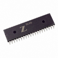
Z85C3008PSG Zilog, Z85C3008PSG Datasheet - Page 140

Z85C3008PSG
Manufacturer Part Number
Z85C3008PSG
Description
IC 8MHZ Z8500 CMOS SCC 40-DIP
Manufacturer
Zilog
Series
SCCr
Specifications of Z85C3008PSG
Processor Type
Z80
Features
Error Detection and Multiprotocol Support
Speed
8MHz
Voltage
5V
Mounting Type
Through Hole
Package / Case
40-DIP (0.620", 15.75mm)
Maximum Operating Temperature
+ 70 C
Minimum Operating Temperature
0 C
Mounting Style
Through Hole
Cpu Speed
8MHz
Digital Ic Case Style
DIP
No. Of Pins
40
Supply Voltage Range
5V
Operating Temperature Range
0°C To +70°C
Svhc
No SVHC (18-Jun-2010)
Base Number
85
Rohs Compliant
Yes
Clock Frequency
8MHz
Lead Free Status / RoHS Status
Lead free / RoHS Compliant
Other names
269-3930
Q2456016A
Z85C3008PSG
Q2456016A
Z85C3008PSG
Available stocks
Company
Part Number
Manufacturer
Quantity
Price
Company:
Part Number:
Z85C3008PSG
Manufacturer:
ZILOG
Quantity:
6 100
Company:
Part Number:
Z85C3008PSG
Manufacturer:
Zilog
Quantity:
6
Company:
Part Number:
Z85C3008PSG
Manufacturer:
TOSHIBA
Quantity:
3 500
Part Number:
Z85C3008PSG
Manufacturer:
ZILOG
Quantity:
20 000
Company:
Part Number:
Z85C3008PSGSCC
Manufacturer:
ZILOG
Quantity:
2
- Current page: 140 of 317
- Download datasheet (4Mb)
UM010901-0601
INPUT/OUTPUT CYCLES
Although Z8500 peripherals are designed to be as
universal as possible, certain timing parameters differ from
the standard Z80 timing. The following sections discuss
the I/O interface for each of the Z80 CPUs and the Z8500
peripherals. Figure 9 depicts logic for the Z80A CPU to
Z8500 peripherals (and Z80B CPU to Z8500A peripherals)
I/O interface as well as the Interrupt Acknowledge
interface. Figures 4 and 7 depict some of the logic used to
interface the Z80H CPU to the Z8500 and Z8500A
peripherals for the I/O and Interrupt Acknowledge
interfaces. The logic required for adding additional Wait
states into the timing flow is not discussed in the following
sections.
Z80A CPU to Z8500 Peripherals
No additional Wait states are necessary during the I/O
cycles, although additional Wait states can be inserted to
compensate for timing delays that are inherent in a
system. Although the Z80A timing parameters indicate a
negative value for data valid prior to /WR, this is a worse
than “worst case” value. This parameter is based upon the
longest (worst case) delay for data available from the
falling edge of the CPU clock minus the shortest (best
case) delay for CPU clock High to /WR low. The negative
value resulting from these two parameters does not occur
because the worst case of one parameter and the best
case of the other do not occur within the same device. This
indicates that the value for data available prior to /WR will
always be greater than zero.
All setup and pulse width times for the Z8500 peripherals
are met by the standard Z80A timing. In determining the
interface necessary, the /CE signal to the Z8500
peripherals is assumed to be the decoded address
qualified with the /IORQ signal.
Figure 4 shows the minimum Z80A CPU to Z8500
peripheral interface timing for I/O cycles. If additional Wait
states are needed, the same number of Wait states can be
inserted for both I/O Read and Write cycles to simplify
interface logic. There are several ways to place the Z80A
CPU into a Wait condition (such as counters or shift
registers to count system clock pulses), depending upon
whether or not the user wants to place Wait states in all
I/O cycles, or only during Z8500 I/O cycles. Tables 3 and
4 list the Z8500 peripheral and the Z80A CPU timing
parameters (respectively) of concern during the I/O cycles.
Tables 5 and 6 list the equations used in determining if
these parameters are satisfied. In generating these
equations and the values obtained from them, the required
number of Wait states was taken into account. The
reference numbers in Tables 3 and 4 refer to the timing
diagram in Figure 4.
Interfacing Z80
®
CPUs to the Z8500 Peripheral Family
Application Note
6-5
6
Related parts for Z85C3008PSG
Image
Part Number
Description
Manufacturer
Datasheet
Request
R

Part Number:
Description:
Manufacturer:
Zilog, Inc.
Datasheet:

Part Number:
Description:
Cmos Scc Serial Communications Controller
Manufacturer:
ZiLOG Semiconductor
Datasheet:

Part Number:
Description:
Communication Controllers, ZILOG INTELLIGENT PERIPHERAL CONTROLLER (ZIP)
Manufacturer:
Zilog, Inc.
Datasheet:

Part Number:
Description:
KIT DEV FOR Z8 ENCORE 16K TO 64K
Manufacturer:
Zilog
Datasheet:

Part Number:
Description:
KIT DEV Z8 ENCORE XP 28-PIN
Manufacturer:
Zilog
Datasheet:

Part Number:
Description:
DEV KIT FOR Z8 ENCORE 8K/4K
Manufacturer:
Zilog
Datasheet:

Part Number:
Description:
KIT DEV Z8 ENCORE XP 28-PIN
Manufacturer:
Zilog
Datasheet:

Part Number:
Description:
DEV KIT FOR Z8 ENCORE 4K TO 8K
Manufacturer:
Zilog
Datasheet:

Part Number:
Description:
CMOS Z8 microcontroller. ROM 16 Kbytes, RAM 256 bytes, speed 16 MHz, 32 lines I/O, 3.0V to 5.5V
Manufacturer:
Zilog, Inc.
Datasheet:

Part Number:
Description:
Low-cost microcontroller. 512 bytes ROM, 61 bytes RAM, 8 MHz
Manufacturer:
Zilog, Inc.
Datasheet:

Part Number:
Description:
Z8 4K OTP Microcontroller
Manufacturer:
Zilog, Inc.
Datasheet:

Part Number:
Description:
CMOS SUPER8 ROMLESS MCU
Manufacturer:
Zilog, Inc.
Datasheet:

Part Number:
Description:
SL1866 CMOSZ8 OTP Microcontroller
Manufacturer:
Zilog, Inc.
Datasheet:


