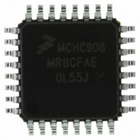
MCHC908MR8CFAE Freescale Semiconductor, MCHC908MR8CFAE Datasheet - Page 345

MCHC908MR8CFAE
Manufacturer Part Number
MCHC908MR8CFAE
Description
IC MCU 8K FLASH 8MHZ PWM 32-LQFP
Manufacturer
Freescale Semiconductor
Series
HC08r
Datasheet
1.MCHC908MR8VFAE.pdf
(372 pages)
Specifications of MCHC908MR8CFAE
Core Processor
HC08
Core Size
8-Bit
Speed
8MHz
Connectivity
SCI
Peripherals
LVD, POR, PWM
Number Of I /o
16
Program Memory Size
8KB (8K x 8)
Program Memory Type
FLASH
Ram Size
256 x 8
Voltage - Supply (vcc/vdd)
4.5 V ~ 5.5 V
Data Converters
A/D 7x10b
Oscillator Type
Internal
Operating Temperature
-40°C ~ 85°C
Package / Case
32-LQFP
Controller Family/series
HC08
No. Of I/o's
16
Ram Memory Size
256Byte
Cpu Speed
8MHz
No. Of Timers
2
Rohs Compliant
Yes
Processor Series
HC08MR
Core
HC08
Data Bus Width
8 bit
Data Ram Size
64 B
Interface Type
SCI, SPI
Maximum Clock Frequency
8 MHz
Number Of Programmable I/os
32
Number Of Timers
4
Operating Supply Voltage
0 V to 5 V
Maximum Operating Temperature
+ 85 C
Mounting Style
SMD/SMT
Development Tools By Supplier
FSICEBASE, M68CBL05CE
Minimum Operating Temperature
- 40 C
On-chip Adc
8 bit, 8 Channel
Lead Free Status / RoHS Status
Lead free / RoHS Compliant
Eeprom Size
-
Lead Free Status / Rohs Status
Details
Available stocks
Company
Part Number
Manufacturer
Quantity
Price
Company:
Part Number:
MCHC908MR8CFAE
Manufacturer:
Freescale Semiconductor
Quantity:
10 000
- Current page: 345 of 372
- Download datasheet (4Mb)
21.7 Memory Characteristics
MC68HC908MR8 — Rev 4.1
Freescale Semiconductor
RAM data retention voltage
FLASH program bus clock frequency
FLASH read bus clock frequency
FLASH page erase time
FLASH mass erase time
FLASH PGM/ERASE to HVEN set up time
FLASH high-voltage hold time
FLASH high-voltage hold time (mass erase)
FLASH program hold time
FLASH program time
FLASH return to read time
FLASH cumulative program HV period
FLASH row erase endurance
FLASH row program endurance
FLASH data retention time
Notes:
1. f
2. If the page erase time is longer than t
3. If the mass erase time is longer than t
4. t
5.
6. The minimum row endurance value specifies each row of the FLASH memory is guaranteed to work for at
7. FLASH endurance is a function of the temperature at which erasure occurs. Typical endurance degrades when the tem-
8. The minimum row endurance value specifies each row of the FLASH memory is guaranteed to work for at
9. The FLASH is guaranteed to retain data over the entire operating temperature range for at least the minimum
10. Freescale performs reliability testing for data retention. These tests are based on samples tested at elevated tempera-
t
memory.
memory.
HVEN to logic 0.
t
least this many erase / program cycles.
perature while erasing is less than 25°C.
least this many erase / program cycles.
time specified.
tures. Due to the higher activation energy of the elevated test temperature, calculated life tests correspond to more than
100 years of operation/storage at 55°C
Read
rcv
HV
HV
is defined as the time it needs before the FLASH can be read after turning off the high voltage charge pump, by clearing
is defined as the cumulative high voltage programming time to the same row before next erase.
must satisfy this condition: t
is defined as the frequency range for which the FLASH memory can be read.
Characteristic
(9)
(6)
nvs
(8)
+ t
nvh
MErase
Erase
+ t
pgs
(Min), there is no erase-disturb, but it reduces the endurance of the FLASH
(Min), there is no erase-disturb, but it reduces the endurance of the FLASH
Electrical Specifications
+ (t
PROG
t
Symbol
MErase
t
f
Erase
Read
t
V
t
t
PROG
rcv
HV
t
t
t
t
nvhl
× 64) ≤ t
RDR
—
nvh
pgs
—
—
—
nvs
(4)
(5)
(1)
(2)
(3)
HV
max.
Min
32k
100
10k
10k
1.3
10
30
—
10
1
1
4
5
5
1
100k
100k
100
Typ
—
—
—
—
—
—
—
—
—
—
—
—
(10)
(7)
(7)
Electrical Specifications
Memory Characteristics
8.4M
Max
40
—
—
—
—
—
—
—
—
—
—
—
—
4
Technical Data
Cycles
Cycles
Years
MHz
Unit
ms
ms
ms
Hz
µs
µs
µs
µs
µs
µs
V
345
Related parts for MCHC908MR8CFAE
Image
Part Number
Description
Manufacturer
Datasheet
Request
R
Part Number:
Description:
Manufacturer:
Freescale Semiconductor, Inc
Datasheet:
Part Number:
Description:
Manufacturer:
Freescale Semiconductor, Inc
Datasheet:
Part Number:
Description:
Manufacturer:
Freescale Semiconductor, Inc
Datasheet:
Part Number:
Description:
Manufacturer:
Freescale Semiconductor, Inc
Datasheet:
Part Number:
Description:
Manufacturer:
Freescale Semiconductor, Inc
Datasheet:
Part Number:
Description:
Manufacturer:
Freescale Semiconductor, Inc
Datasheet:
Part Number:
Description:
Manufacturer:
Freescale Semiconductor, Inc
Datasheet:
Part Number:
Description:
Manufacturer:
Freescale Semiconductor, Inc
Datasheet:
Part Number:
Description:
Manufacturer:
Freescale Semiconductor, Inc
Datasheet:
Part Number:
Description:
Manufacturer:
Freescale Semiconductor, Inc
Datasheet:
Part Number:
Description:
Manufacturer:
Freescale Semiconductor, Inc
Datasheet:
Part Number:
Description:
Manufacturer:
Freescale Semiconductor, Inc
Datasheet:
Part Number:
Description:
Manufacturer:
Freescale Semiconductor, Inc
Datasheet:
Part Number:
Description:
Manufacturer:
Freescale Semiconductor, Inc
Datasheet:
Part Number:
Description:
Manufacturer:
Freescale Semiconductor, Inc
Datasheet:


