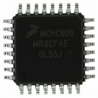
MCHC908MR8CFAE Freescale Semiconductor, MCHC908MR8CFAE Datasheet - Page 213

MCHC908MR8CFAE
Manufacturer Part Number
MCHC908MR8CFAE
Description
IC MCU 8K FLASH 8MHZ PWM 32-LQFP
Manufacturer
Freescale Semiconductor
Series
HC08r
Datasheet
1.MCHC908MR8VFAE.pdf
(372 pages)
Specifications of MCHC908MR8CFAE
Core Processor
HC08
Core Size
8-Bit
Speed
8MHz
Connectivity
SCI
Peripherals
LVD, POR, PWM
Number Of I /o
16
Program Memory Size
8KB (8K x 8)
Program Memory Type
FLASH
Ram Size
256 x 8
Voltage - Supply (vcc/vdd)
4.5 V ~ 5.5 V
Data Converters
A/D 7x10b
Oscillator Type
Internal
Operating Temperature
-40°C ~ 85°C
Package / Case
32-LQFP
Controller Family/series
HC08
No. Of I/o's
16
Ram Memory Size
256Byte
Cpu Speed
8MHz
No. Of Timers
2
Rohs Compliant
Yes
Processor Series
HC08MR
Core
HC08
Data Bus Width
8 bit
Data Ram Size
64 B
Interface Type
SCI, SPI
Maximum Clock Frequency
8 MHz
Number Of Programmable I/os
32
Number Of Timers
4
Operating Supply Voltage
0 V to 5 V
Maximum Operating Temperature
+ 85 C
Mounting Style
SMD/SMT
Development Tools By Supplier
FSICEBASE, M68CBL05CE
Minimum Operating Temperature
- 40 C
On-chip Adc
8 bit, 8 Channel
Lead Free Status / RoHS Status
Lead free / RoHS Compliant
Eeprom Size
-
Lead Free Status / Rohs Status
Details
Available stocks
Company
Part Number
Manufacturer
Quantity
Price
Company:
Part Number:
MCHC908MR8CFAE
Manufacturer:
Freescale Semiconductor
Quantity:
10 000
- Current page: 213 of 372
- Download datasheet (4Mb)
11.9.1 TIMA Clock Pin (PTB2/TCLKA)
11.9.2 TIMA Channel I/O Pins (PTB3/TCH0A–PTB4/TCH1A)
11.10 I/O Registers
MC68HC908MR8 — Rev 4.1
Freescale Semiconductor
PTB2/TCLKA is an external clock input that can be the clock source for
the TIMA counter instead of the prescaled internal bus clock. Select the
PTB2/TCLKA input by writing logic 1s to the three prescaler select bits,
PS[2:0] (see
minimum TCLK pulse width, TCLKLMIN or TCLKHMIN, is:
The maximum TCLK frequency is the least: 4 MHz or bus frequency ÷ 2.
PTB2/TCLKA is available as a general-purpose I/O pin or ADC channel
when not used as the TIMA clock input. When the PTB2/TCLKA pin is
the TIMA clock input, it is an input regardless of the state of the DDRB2
bit in data direction register B.
Each channel I/O pin is programmable independently as an input
capture pin or an output compare pin. PTB3/TCH0A and PTB3/TCH1A
can be configured as buffered output compare or buffered PWM pins.
These I/O registers control and monitor TIMA operation:
•
•
•
•
•
TIMA status and control register (TASC)
TIMA control registers (TACNTH–TACNTL)
TIMA counter modulo registers (TAMODH–TAMODL)
TIMA channel status and control registers (TASC0 and TASC1)
TIMA channel registers (TACH0H–TACH0L and
TACH1H–TACH1L)
11.10.1 TIMA Status and Control
Timer Interface A (TIMA)
------------------------------------ -
bus frequency
1
+
t
su
Register). The
Timer Interface A (TIMA)
Technical Data
I/O Registers
213
Related parts for MCHC908MR8CFAE
Image
Part Number
Description
Manufacturer
Datasheet
Request
R
Part Number:
Description:
Manufacturer:
Freescale Semiconductor, Inc
Datasheet:
Part Number:
Description:
Manufacturer:
Freescale Semiconductor, Inc
Datasheet:
Part Number:
Description:
Manufacturer:
Freescale Semiconductor, Inc
Datasheet:
Part Number:
Description:
Manufacturer:
Freescale Semiconductor, Inc
Datasheet:
Part Number:
Description:
Manufacturer:
Freescale Semiconductor, Inc
Datasheet:
Part Number:
Description:
Manufacturer:
Freescale Semiconductor, Inc
Datasheet:
Part Number:
Description:
Manufacturer:
Freescale Semiconductor, Inc
Datasheet:
Part Number:
Description:
Manufacturer:
Freescale Semiconductor, Inc
Datasheet:
Part Number:
Description:
Manufacturer:
Freescale Semiconductor, Inc
Datasheet:
Part Number:
Description:
Manufacturer:
Freescale Semiconductor, Inc
Datasheet:
Part Number:
Description:
Manufacturer:
Freescale Semiconductor, Inc
Datasheet:
Part Number:
Description:
Manufacturer:
Freescale Semiconductor, Inc
Datasheet:
Part Number:
Description:
Manufacturer:
Freescale Semiconductor, Inc
Datasheet:
Part Number:
Description:
Manufacturer:
Freescale Semiconductor, Inc
Datasheet:
Part Number:
Description:
Manufacturer:
Freescale Semiconductor, Inc
Datasheet:


