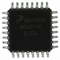
MCHC908MR8CFAE Freescale Semiconductor, MCHC908MR8CFAE Datasheet - Page 165

MCHC908MR8CFAE
Manufacturer Part Number
MCHC908MR8CFAE
Description
IC MCU 8K FLASH 8MHZ PWM 32-LQFP
Manufacturer
Freescale Semiconductor
Series
HC08r
Datasheet
1.MCHC908MR8VFAE.pdf
(372 pages)
Specifications of MCHC908MR8CFAE
Core Processor
HC08
Core Size
8-Bit
Speed
8MHz
Connectivity
SCI
Peripherals
LVD, POR, PWM
Number Of I /o
16
Program Memory Size
8KB (8K x 8)
Program Memory Type
FLASH
Ram Size
256 x 8
Voltage - Supply (vcc/vdd)
4.5 V ~ 5.5 V
Data Converters
A/D 7x10b
Oscillator Type
Internal
Operating Temperature
-40°C ~ 85°C
Package / Case
32-LQFP
Controller Family/series
HC08
No. Of I/o's
16
Ram Memory Size
256Byte
Cpu Speed
8MHz
No. Of Timers
2
Rohs Compliant
Yes
Processor Series
HC08MR
Core
HC08
Data Bus Width
8 bit
Data Ram Size
64 B
Interface Type
SCI, SPI
Maximum Clock Frequency
8 MHz
Number Of Programmable I/os
32
Number Of Timers
4
Operating Supply Voltage
0 V to 5 V
Maximum Operating Temperature
+ 85 C
Mounting Style
SMD/SMT
Development Tools By Supplier
FSICEBASE, M68CBL05CE
Minimum Operating Temperature
- 40 C
On-chip Adc
8 bit, 8 Channel
Lead Free Status / RoHS Status
Lead free / RoHS Compliant
Eeprom Size
-
Lead Free Status / Rohs Status
Details
Available stocks
Company
Part Number
Manufacturer
Quantity
Price
Company:
Part Number:
MCHC908MR8CFAE
Manufacturer:
Freescale Semiconductor
Quantity:
10 000
- Current page: 165 of 372
- Download datasheet (4Mb)
9.7.1.1 Fault Pin Filter
9.7.1.2 Automatic Mode
MC68HC908MR8 — Rev 4.1
Freescale Semiconductor
non-fault condition to facilitate the use of PORTC as an output pin and
not interfere with the PWM generator. To regain the fault capability for
the respective fault input pin, clear the PORTC data direction register bit
for that pin.
Additionally, when the device is reset, by default, PORTC is configured
as an input. If either bit(s) of PORTC is intended to be used as an output,
the logic state of the driven device’s input is indeterminate. The state of
the driven device, if at a logic one will drive the respective bit of PORTC
input high, thus causing a fault to be input to the respective PORTC input
and to the PWM module.
After setting the PORTC data direction register, clear the respective fault
bits by writing a 1 to bit(s) 0 and or bit 6 in the FTACK Fault Acknowledge
Register (FTACK) and Fault Status Registers (FSR), based on which
PORTC bits that are used as output(s).
The two fault pins incorporate a filter to assist in determining a genuine
fault condition. After a fault pin has been logic low for one CPU cycle, a
rising edge (logic high) will be synchronously sampled once per CPU
cycle for two cycles. If both samples are detected logic high, the
corresponding FPIN bit and FFLAG bit will be set. The FPIN bit will
remain set until the corresponding fault pin is logic low and
synchronously sampled once in the following CPU cycle.
In automatic mode, the PWM(s) are disabled immediately once a filtered
fault condition is detected (logic high). The PWM(s) remain disabled until
the filtered fault condition is cleared (logic low) and a new PWM cycle
begins as shown in
event bit will not enable the PWMs in automatic mode.
Pulse-Width Modulator for Motor Control (PWMMC)
Figure
9-24. Clearing the corresponding FFLAGx
Pulse-Width Modulator for Motor Control (PWMMC)
Fault Protection
Technical Data
165
Related parts for MCHC908MR8CFAE
Image
Part Number
Description
Manufacturer
Datasheet
Request
R
Part Number:
Description:
Manufacturer:
Freescale Semiconductor, Inc
Datasheet:
Part Number:
Description:
Manufacturer:
Freescale Semiconductor, Inc
Datasheet:
Part Number:
Description:
Manufacturer:
Freescale Semiconductor, Inc
Datasheet:
Part Number:
Description:
Manufacturer:
Freescale Semiconductor, Inc
Datasheet:
Part Number:
Description:
Manufacturer:
Freescale Semiconductor, Inc
Datasheet:
Part Number:
Description:
Manufacturer:
Freescale Semiconductor, Inc
Datasheet:
Part Number:
Description:
Manufacturer:
Freescale Semiconductor, Inc
Datasheet:
Part Number:
Description:
Manufacturer:
Freescale Semiconductor, Inc
Datasheet:
Part Number:
Description:
Manufacturer:
Freescale Semiconductor, Inc
Datasheet:
Part Number:
Description:
Manufacturer:
Freescale Semiconductor, Inc
Datasheet:
Part Number:
Description:
Manufacturer:
Freescale Semiconductor, Inc
Datasheet:
Part Number:
Description:
Manufacturer:
Freescale Semiconductor, Inc
Datasheet:
Part Number:
Description:
Manufacturer:
Freescale Semiconductor, Inc
Datasheet:
Part Number:
Description:
Manufacturer:
Freescale Semiconductor, Inc
Datasheet:
Part Number:
Description:
Manufacturer:
Freescale Semiconductor, Inc
Datasheet:


