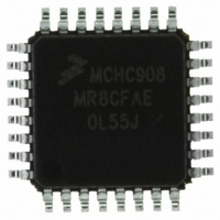
MCHC908MR8CFAE Freescale Semiconductor, MCHC908MR8CFAE Datasheet - Page 263

MCHC908MR8CFAE
Manufacturer Part Number
MCHC908MR8CFAE
Description
IC MCU 8K FLASH 8MHZ PWM 32-LQFP
Manufacturer
Freescale Semiconductor
Series
HC08r
Datasheet
1.MCHC908MR8VFAE.pdf
(372 pages)
Specifications of MCHC908MR8CFAE
Core Processor
HC08
Core Size
8-Bit
Speed
8MHz
Connectivity
SCI
Peripherals
LVD, POR, PWM
Number Of I /o
16
Program Memory Size
8KB (8K x 8)
Program Memory Type
FLASH
Ram Size
256 x 8
Voltage - Supply (vcc/vdd)
4.5 V ~ 5.5 V
Data Converters
A/D 7x10b
Oscillator Type
Internal
Operating Temperature
-40°C ~ 85°C
Package / Case
32-LQFP
Controller Family/series
HC08
No. Of I/o's
16
Ram Memory Size
256Byte
Cpu Speed
8MHz
No. Of Timers
2
Rohs Compliant
Yes
Processor Series
HC08MR
Core
HC08
Data Bus Width
8 bit
Data Ram Size
64 B
Interface Type
SCI, SPI
Maximum Clock Frequency
8 MHz
Number Of Programmable I/os
32
Number Of Timers
4
Operating Supply Voltage
0 V to 5 V
Maximum Operating Temperature
+ 85 C
Mounting Style
SMD/SMT
Development Tools By Supplier
FSICEBASE, M68CBL05CE
Minimum Operating Temperature
- 40 C
On-chip Adc
8 bit, 8 Channel
Lead Free Status / RoHS Status
Lead free / RoHS Compliant
Eeprom Size
-
Lead Free Status / Rohs Status
Details
Available stocks
Company
Part Number
Manufacturer
Quantity
Price
Company:
Part Number:
MCHC908MR8CFAE
Manufacturer:
Freescale Semiconductor
Quantity:
10 000
- Current page: 263 of 372
- Download datasheet (4Mb)
13.8 I/O Signals
13.8.1 PTE2/TxD (Transmit Data)
13.8.2 PTB0/RxD (Receive Data)
13.9 I/O Registers
MC68HC908MR8 — Rev 4.1
Freescale Semiconductor
Port B shares two of its pins with the SCI module. The two SCI I/O pins
are:
The PTB1/TxD pin is the serial data output from the SCI transmitter. The
SCI shares the PTB1/TxD pin with port B. When the SCI is enabled, the
PTB1/TxD pin is an output regardless of the state of the DDRF1 bit in
data direction register B (DDRB).
The PTB0/RxD pin is the serial data input to the SCI receiver. The SCI
shares the PTB0/RxD pin with port B. When the SCI is enabled, the
PTB0/RxD pin is an input regardless of the state of the DDRB0 bit in data
direction register B (DDRB).
These I/O registers control and monitor SCI operation:
•
•
•
•
•
•
•
•
•
PTB1/TxD — Transmit data
PTB0/RxD — Receive data
SCI control register 1 (SCC1)
SCI control register 2 (SCC2)
SCI control register 3 (SCC3)
SCI status register 1 (SCS1)
SCI status register 2 (SCS2)
SCI data register (SCDR)
SCI baud rate register (SCBR)
Serial Communications Interface (SCI)
Serial Communications Interface (SCI)
Technical Data
I/O Signals
263
Related parts for MCHC908MR8CFAE
Image
Part Number
Description
Manufacturer
Datasheet
Request
R
Part Number:
Description:
Manufacturer:
Freescale Semiconductor, Inc
Datasheet:
Part Number:
Description:
Manufacturer:
Freescale Semiconductor, Inc
Datasheet:
Part Number:
Description:
Manufacturer:
Freescale Semiconductor, Inc
Datasheet:
Part Number:
Description:
Manufacturer:
Freescale Semiconductor, Inc
Datasheet:
Part Number:
Description:
Manufacturer:
Freescale Semiconductor, Inc
Datasheet:
Part Number:
Description:
Manufacturer:
Freescale Semiconductor, Inc
Datasheet:
Part Number:
Description:
Manufacturer:
Freescale Semiconductor, Inc
Datasheet:
Part Number:
Description:
Manufacturer:
Freescale Semiconductor, Inc
Datasheet:
Part Number:
Description:
Manufacturer:
Freescale Semiconductor, Inc
Datasheet:
Part Number:
Description:
Manufacturer:
Freescale Semiconductor, Inc
Datasheet:
Part Number:
Description:
Manufacturer:
Freescale Semiconductor, Inc
Datasheet:
Part Number:
Description:
Manufacturer:
Freescale Semiconductor, Inc
Datasheet:
Part Number:
Description:
Manufacturer:
Freescale Semiconductor, Inc
Datasheet:
Part Number:
Description:
Manufacturer:
Freescale Semiconductor, Inc
Datasheet:
Part Number:
Description:
Manufacturer:
Freescale Semiconductor, Inc
Datasheet:


