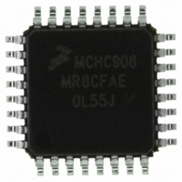
MCHC908MR8CFAE Freescale Semiconductor, MCHC908MR8CFAE Datasheet - Page 113

MCHC908MR8CFAE
Manufacturer Part Number
MCHC908MR8CFAE
Description
IC MCU 8K FLASH 8MHZ PWM 32-LQFP
Manufacturer
Freescale Semiconductor
Series
HC08r
Datasheet
1.MCHC908MR8VFAE.pdf
(372 pages)
Specifications of MCHC908MR8CFAE
Core Processor
HC08
Core Size
8-Bit
Speed
8MHz
Connectivity
SCI
Peripherals
LVD, POR, PWM
Number Of I /o
16
Program Memory Size
8KB (8K x 8)
Program Memory Type
FLASH
Ram Size
256 x 8
Voltage - Supply (vcc/vdd)
4.5 V ~ 5.5 V
Data Converters
A/D 7x10b
Oscillator Type
Internal
Operating Temperature
-40°C ~ 85°C
Package / Case
32-LQFP
Controller Family/series
HC08
No. Of I/o's
16
Ram Memory Size
256Byte
Cpu Speed
8MHz
No. Of Timers
2
Rohs Compliant
Yes
Processor Series
HC08MR
Core
HC08
Data Bus Width
8 bit
Data Ram Size
64 B
Interface Type
SCI, SPI
Maximum Clock Frequency
8 MHz
Number Of Programmable I/os
32
Number Of Timers
4
Operating Supply Voltage
0 V to 5 V
Maximum Operating Temperature
+ 85 C
Mounting Style
SMD/SMT
Development Tools By Supplier
FSICEBASE, M68CBL05CE
Minimum Operating Temperature
- 40 C
On-chip Adc
8 bit, 8 Channel
Lead Free Status / RoHS Status
Lead free / RoHS Compliant
Eeprom Size
-
Lead Free Status / Rohs Status
Details
Available stocks
Company
Part Number
Manufacturer
Quantity
Price
Company:
Part Number:
MCHC908MR8CFAE
Manufacturer:
Freescale Semiconductor
Quantity:
10 000
- Current page: 113 of 372
- Download datasheet (4Mb)
8.4 Functional Description
8.4.1 Crystal Oscillator Circuit
MC68HC908MR8 — Rev 4.1
Freescale Semiconductor
The CGM consists of three major submodules:
Figure 8-1
The crystal oscillator circuit consists of an inverting amplifier and an
external crystal. The OSC1 pin is the input to the amplifier and the OSC2
pin is the output. The SIMOSCEN signal from the system integration
module (SIM) enables the crystal oscillator circuit.
The CGMXCLK signal is the output of the crystal oscillator circuit and
runs at a rate equal to the crystal frequency. CGMXCLK is then buffered
to produce CGMRCLK, the PLL reference clock.
CGMXCLK can be used by other modules which require precise timing
for operation. The duty cycle of CGMXCLK is not guaranteed to be
50 percent and depends on external factors, including the crystal and
related external components.
An externally generated clock also can feed the OSC1 pin of the crystal
oscillator circuit. Connect the external clock to the OSC1 pin and let the
OSC2 pin float.
1. Crystal oscillator circuit — The crystal oscillator circuit generates
2. Phase-locked loop (PLL) — The PLL generates the
3. Base clock selector circuit — This software-controlled circuit
the constant crystal frequency clock, CGMXCLK.
programmable VCO frequency clock, CGMVCLK.
selects either CGMXCLK divided by two or the VCO clock,
CGMVCLK, divided by two as the base clock, CGMOUT. The SIM
derives the system clocks from CGMOUT.
Clock Generator Module (CGM)
shows the structure of the CGM.
Clock Generator Module (CGM)
Functional Description
Technical Data
113
Related parts for MCHC908MR8CFAE
Image
Part Number
Description
Manufacturer
Datasheet
Request
R
Part Number:
Description:
Manufacturer:
Freescale Semiconductor, Inc
Datasheet:
Part Number:
Description:
Manufacturer:
Freescale Semiconductor, Inc
Datasheet:
Part Number:
Description:
Manufacturer:
Freescale Semiconductor, Inc
Datasheet:
Part Number:
Description:
Manufacturer:
Freescale Semiconductor, Inc
Datasheet:
Part Number:
Description:
Manufacturer:
Freescale Semiconductor, Inc
Datasheet:
Part Number:
Description:
Manufacturer:
Freescale Semiconductor, Inc
Datasheet:
Part Number:
Description:
Manufacturer:
Freescale Semiconductor, Inc
Datasheet:
Part Number:
Description:
Manufacturer:
Freescale Semiconductor, Inc
Datasheet:
Part Number:
Description:
Manufacturer:
Freescale Semiconductor, Inc
Datasheet:
Part Number:
Description:
Manufacturer:
Freescale Semiconductor, Inc
Datasheet:
Part Number:
Description:
Manufacturer:
Freescale Semiconductor, Inc
Datasheet:
Part Number:
Description:
Manufacturer:
Freescale Semiconductor, Inc
Datasheet:
Part Number:
Description:
Manufacturer:
Freescale Semiconductor, Inc
Datasheet:
Part Number:
Description:
Manufacturer:
Freescale Semiconductor, Inc
Datasheet:
Part Number:
Description:
Manufacturer:
Freescale Semiconductor, Inc
Datasheet:


