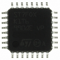
ST7FOXK1T6 STMicroelectronics, ST7FOXK1T6 Datasheet - Page 46

ST7FOXK1T6
Manufacturer Part Number
ST7FOXK1T6
Description
IC MCU 8BIT 1V FLASH MEM 32LQFP
Manufacturer
STMicroelectronics
Series
ST7r
Datasheet
1.ST7FOXF1M6.pdf
(226 pages)
Specifications of ST7FOXK1T6
Core Processor
ST7
Core Size
8-Bit
Speed
8MHz
Connectivity
I²C
Peripherals
LVD, POR, PWM, WDT
Number Of I /o
24
Program Memory Size
4KB (4K x 8)
Program Memory Type
FLASH
Ram Size
384 x 8
Voltage - Supply (vcc/vdd)
4.5 V ~ 5.5 V
Data Converters
A/D 10x10b
Oscillator Type
Internal
Operating Temperature
-40°C ~ 85°C
Package / Case
32-LQFP
Processor Series
ST7FOXx
Core
ST7
Data Bus Width
8 bit
Data Ram Size
384 B
Interface Type
I2C
Maximum Clock Frequency
8 MHz
Number Of Programmable I/os
24
Number Of Timers
4
Maximum Operating Temperature
+ 85 C
Mounting Style
SMD/SMT
Development Tools By Supplier
ST7FLITE-SK/RAIS, STX-RLINK
Minimum Operating Temperature
- 40 C
On-chip Adc
10 bit, 1 Channel
For Use With
497-5049 - KIT STARTER RAISONANCE ST7FLITE
Lead Free Status / RoHS Status
Lead free / RoHS Compliant
Eeprom Size
-
Lead Free Status / Rohs Status
Details
Other names
497-6336
Available stocks
Company
Part Number
Manufacturer
Quantity
Price
Company:
Part Number:
ST7FOXK1T6
Manufacturer:
STMicroelectronics
Quantity:
10 000
Company:
Part Number:
ST7FOXK1T6TR
Manufacturer:
STMicroelectronics
Quantity:
10 000
- Current page: 46 of 226
- Download datasheet (4Mb)
Supply, reset and clock management
6.5
6.5.1
Note:
6.5.2
46/226
Register description
RC calibration control/status register (RCC_CSR)
Reset value: 0000 0000 (00h)
Bits 7:2 = Reserved, forced by hardware to 0
Bit 1 = RCCLAT Latch Access Transfer bit: this bit is set by software.
Bit 0 = RCCPGM Programming Control and Status bit
If the RCCPGM bit is cleared during the programming cycle, the memory data is not
guaranteed.
Main Clock Control/Status Register (MCCSR)
Reset value: 0000 0000 (00h)
Bits 7:2 = Reserved, must be kept cleared.
Bit 1 = MCO Main Clock Out enable bit
Bit 0 = SMS Slow mode selection bit
0: Read mode
1: Write mode
It is cleared by hardware at the end of the programming cycle. It can only be cleared by
software if the RCCPGM bit is cleared
This bit is set by software to begin the programming cycle. At the end of the
programming cycle, this bit is cleared by hardware.
0: Programming finished or not yet started
1: Programming cycle is in progress
This bit is read/write by software and cleared by hardware after a reset. This bit allows
to enable the MCO output clock.
0: MCO clock disabled, I/O port free for general purpose I/O.
1: MCO clock enabled.
This bit is read/write by software and cleared by hardware after a reset. This bit selects
the input clock f
0: Normal mode (f
1: Slow mode (f
7
0
7
0
0
0
OSC
CPU =
CPU =
or f
f
OSC
0
0
OSC
f
OSC
/32)
/32.
0
0
Read/write
Read/write
0
0
ST7FOXF1, ST7FOXK1, ST7FOXK2
0
0
RCCLAT
MCO
RCCPGM
SMS
0
0
Related parts for ST7FOXK1T6
Image
Part Number
Description
Manufacturer
Datasheet
Request
R

Part Number:
Description:
STMicroelectronics [RIPPLE-CARRY BINARY COUNTER/DIVIDERS]
Manufacturer:
STMicroelectronics
Datasheet:

Part Number:
Description:
STMicroelectronics [LIQUID-CRYSTAL DISPLAY DRIVERS]
Manufacturer:
STMicroelectronics
Datasheet:

Part Number:
Description:
BOARD EVAL FOR MEMS SENSORS
Manufacturer:
STMicroelectronics
Datasheet:

Part Number:
Description:
NPN TRANSISTOR POWER MODULE
Manufacturer:
STMicroelectronics
Datasheet:

Part Number:
Description:
TURBOSWITCH ULTRA-FAST HIGH VOLTAGE DIODE
Manufacturer:
STMicroelectronics
Datasheet:

Part Number:
Description:
Manufacturer:
STMicroelectronics
Datasheet:

Part Number:
Description:
DIODE / SCR MODULE
Manufacturer:
STMicroelectronics
Datasheet:

Part Number:
Description:
DIODE / SCR MODULE
Manufacturer:
STMicroelectronics
Datasheet:

Part Number:
Description:
Search -----> STE16N100
Manufacturer:
STMicroelectronics
Datasheet:

Part Number:
Description:
Search ---> STE53NA50
Manufacturer:
STMicroelectronics
Datasheet:

Part Number:
Description:
NPN Transistor Power Module
Manufacturer:
STMicroelectronics
Datasheet:

Part Number:
Description:
DIODE / SCR MODULE
Manufacturer:
STMicroelectronics
Datasheet:


