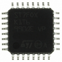
ST7FOXK1T6 STMicroelectronics, ST7FOXK1T6 Datasheet - Page 209

ST7FOXK1T6
Manufacturer Part Number
ST7FOXK1T6
Description
IC MCU 8BIT 1V FLASH MEM 32LQFP
Manufacturer
STMicroelectronics
Series
ST7r
Datasheet
1.ST7FOXF1M6.pdf
(226 pages)
Specifications of ST7FOXK1T6
Core Processor
ST7
Core Size
8-Bit
Speed
8MHz
Connectivity
I²C
Peripherals
LVD, POR, PWM, WDT
Number Of I /o
24
Program Memory Size
4KB (4K x 8)
Program Memory Type
FLASH
Ram Size
384 x 8
Voltage - Supply (vcc/vdd)
4.5 V ~ 5.5 V
Data Converters
A/D 10x10b
Oscillator Type
Internal
Operating Temperature
-40°C ~ 85°C
Package / Case
32-LQFP
Processor Series
ST7FOXx
Core
ST7
Data Bus Width
8 bit
Data Ram Size
384 B
Interface Type
I2C
Maximum Clock Frequency
8 MHz
Number Of Programmable I/os
24
Number Of Timers
4
Maximum Operating Temperature
+ 85 C
Mounting Style
SMD/SMT
Development Tools By Supplier
ST7FLITE-SK/RAIS, STX-RLINK
Minimum Operating Temperature
- 40 C
On-chip Adc
10 bit, 1 Channel
For Use With
497-5049 - KIT STARTER RAISONANCE ST7FLITE
Lead Free Status / RoHS Status
Lead free / RoHS Compliant
Eeprom Size
-
Lead Free Status / Rohs Status
Details
Other names
497-6336
Available stocks
Company
Part Number
Manufacturer
Quantity
Price
Company:
Part Number:
ST7FOXK1T6
Manufacturer:
STMicroelectronics
Quantity:
10 000
Company:
Part Number:
ST7FOXK1T6TR
Manufacturer:
STMicroelectronics
Quantity:
10 000
- Current page: 209 of 226
- Download datasheet (4Mb)
ST7FOXF1, ST7FOXK1, ST7FOXK2
12.11
Table 90.
1. Unless otherwise specified, typical data are based on T
2. Any added external serial resistor will downgrade the ADC accuracy (especially for resistance greater than the maximum
3. The stabilization time of the A/D converter is masked by the first t
Symbol
C
t
R
f
V
t
STAB
ADC
ADC
guidelines and are not tested.
value). Data guaranteed by Design, not tested in production.
valid.
ADC
AIN
AIN
Conversion time (Sample+Hold)
- Sample capacitor loading time
Stabilization time after ADC
10-bit ADC characteristics
Subject to general operating condition for V
ADC characteristics
Figure 91. Typical application with ADC
Conversion voltage range
Internal sample and hold
- Hold conversion time
External input resistor
ADC clock frequency
V
AIN
Parameter
capacitor
enable
R
AIN
AINx
4.5 V ≤ V
f
CPU
V
DD
= 8 MHz, f
A
= 25 °C and V
DD
= 5 V, f
Conditions
≤ 5.5 V, f
V
LOAD
ADC
DD
DD
ADC
= 4 MHz
, f
V
0.6 V
V
0.6 V
. The first conversion after the enable is then always
= 4 MHz
T
T
ADC
DD
OSC
-V
= 2 MHz
SS
, and T
= 5 V. They are given only as design
I
±1 µA
L
A
V
unless otherwise specified.
Min
SSA
Electrical characteristics
Typ
10-Bit A/D
Conversion
0
3.5
10
6
4
(3)
(1)
10k
V
8k
Max
DDA
4
ST7xxx
(2)
(2)
209/226
1/f
C
MHz
Unit
ADC
pF
µs
Ω
V
ADC
Related parts for ST7FOXK1T6
Image
Part Number
Description
Manufacturer
Datasheet
Request
R

Part Number:
Description:
STMicroelectronics [RIPPLE-CARRY BINARY COUNTER/DIVIDERS]
Manufacturer:
STMicroelectronics
Datasheet:

Part Number:
Description:
STMicroelectronics [LIQUID-CRYSTAL DISPLAY DRIVERS]
Manufacturer:
STMicroelectronics
Datasheet:

Part Number:
Description:
BOARD EVAL FOR MEMS SENSORS
Manufacturer:
STMicroelectronics
Datasheet:

Part Number:
Description:
NPN TRANSISTOR POWER MODULE
Manufacturer:
STMicroelectronics
Datasheet:

Part Number:
Description:
TURBOSWITCH ULTRA-FAST HIGH VOLTAGE DIODE
Manufacturer:
STMicroelectronics
Datasheet:

Part Number:
Description:
Manufacturer:
STMicroelectronics
Datasheet:

Part Number:
Description:
DIODE / SCR MODULE
Manufacturer:
STMicroelectronics
Datasheet:

Part Number:
Description:
DIODE / SCR MODULE
Manufacturer:
STMicroelectronics
Datasheet:

Part Number:
Description:
Search -----> STE16N100
Manufacturer:
STMicroelectronics
Datasheet:

Part Number:
Description:
Search ---> STE53NA50
Manufacturer:
STMicroelectronics
Datasheet:

Part Number:
Description:
NPN Transistor Power Module
Manufacturer:
STMicroelectronics
Datasheet:

Part Number:
Description:
DIODE / SCR MODULE
Manufacturer:
STMicroelectronics
Datasheet:


