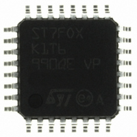
ST7FOXK1T6 STMicroelectronics, ST7FOXK1T6 Datasheet - Page 168

ST7FOXK1T6
Manufacturer Part Number
ST7FOXK1T6
Description
IC MCU 8BIT 1V FLASH MEM 32LQFP
Manufacturer
STMicroelectronics
Series
ST7r
Datasheet
1.ST7FOXF1M6.pdf
(226 pages)
Specifications of ST7FOXK1T6
Core Processor
ST7
Core Size
8-Bit
Speed
8MHz
Connectivity
I²C
Peripherals
LVD, POR, PWM, WDT
Number Of I /o
24
Program Memory Size
4KB (4K x 8)
Program Memory Type
FLASH
Ram Size
384 x 8
Voltage - Supply (vcc/vdd)
4.5 V ~ 5.5 V
Data Converters
A/D 10x10b
Oscillator Type
Internal
Operating Temperature
-40°C ~ 85°C
Package / Case
32-LQFP
Processor Series
ST7FOXx
Core
ST7
Data Bus Width
8 bit
Data Ram Size
384 B
Interface Type
I2C
Maximum Clock Frequency
8 MHz
Number Of Programmable I/os
24
Number Of Timers
4
Maximum Operating Temperature
+ 85 C
Mounting Style
SMD/SMT
Development Tools By Supplier
ST7FLITE-SK/RAIS, STX-RLINK
Minimum Operating Temperature
- 40 C
On-chip Adc
10 bit, 1 Channel
For Use With
497-5049 - KIT STARTER RAISONANCE ST7FLITE
Lead Free Status / RoHS Status
Lead free / RoHS Compliant
Eeprom Size
-
Lead Free Status / Rohs Status
Details
Other names
497-6336
Available stocks
Company
Part Number
Manufacturer
Quantity
Price
Company:
Part Number:
ST7FOXK1T6
Manufacturer:
STMicroelectronics
Quantity:
10 000
Company:
Part Number:
ST7FOXK1T6TR
Manufacturer:
STMicroelectronics
Quantity:
10 000
On-chip peripherals
10.6.9
168/226
Register description
SPI Control register (SPICR)
Reset value: 0000 xxxx (0xh)
Bit 7 = SPIE Serial Peripheral interrupt enable.
Bit 6 = SPE Serial Peripheral output enable.
Bit 5 = SPR2 Divider enable.
Bit 4 = MSTR Master mode.
Bit 3 = CPOL Clock polarity.
SPIE
This bit is set and cleared by software.
0: Interrupt is inhibited
1: An SPI interrupt is generated whenever an End of Transfer event, Master Mode Fault
or Overrun error occurs (SPIF = 1, MODF = 1 or OVR = 1 in the SPICSR register)
This bit is set and cleared by software. It is also cleared by hardware when, in master
mode, SS = 0 (see
reset, so the SPI peripheral is not initially connected to the external pins.
0: I/O pins free for general purpose I/O
1: SPI I/O pin alternate functions enabled
This bit is set and cleared by software and is cleared by reset. It is used with the
SPR[1:0] bits to set the baud rate. Refer to
0: Divider by 2 enabled
1: Divider by 2 disabled
This bit has no effect in slave mode.
This bit is set and cleared by software. It is also cleared by hardware when, in master
mode, SS = 0 (see
0: Slave mode
1: Master mode. The function of the SCK pin changes from an input to an output and
the functions of the MISO and MOSI pins are reversed.
This bit is set and cleared by software. This bit determines the idle state of the serial
Clock. The CPOL bit affects both the master and slave modes.
0: SCK pin has a low level idle state
1: SCK pin has a high level idle state
If CPOL is changed at the communication byte boundaries, the SPI must be disabled
by resetting the SPE bit.
7
SPE
Section : Master mode fault
Section : Master mode fault
SPR2
MSTR
Read / Write
Table 52: SPI Master mode SCK
CPOL
(MODF)). The SPE bit is cleared by
(MODF)).
ST7FOXF1, ST7FOXK1, ST7FOXK2
CPHA
SPR1
Frequency.
SPR0
0


