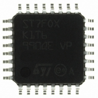
ST7FOXK1T6 STMicroelectronics, ST7FOXK1T6 Datasheet - Page 35

ST7FOXK1T6
Manufacturer Part Number
ST7FOXK1T6
Description
IC MCU 8BIT 1V FLASH MEM 32LQFP
Manufacturer
STMicroelectronics
Series
ST7r
Datasheet
1.ST7FOXF1M6.pdf
(226 pages)
Specifications of ST7FOXK1T6
Core Processor
ST7
Core Size
8-Bit
Speed
8MHz
Connectivity
I²C
Peripherals
LVD, POR, PWM, WDT
Number Of I /o
24
Program Memory Size
4KB (4K x 8)
Program Memory Type
FLASH
Ram Size
384 x 8
Voltage - Supply (vcc/vdd)
4.5 V ~ 5.5 V
Data Converters
A/D 10x10b
Oscillator Type
Internal
Operating Temperature
-40°C ~ 85°C
Package / Case
32-LQFP
Processor Series
ST7FOXx
Core
ST7
Data Bus Width
8 bit
Data Ram Size
384 B
Interface Type
I2C
Maximum Clock Frequency
8 MHz
Number Of Programmable I/os
24
Number Of Timers
4
Maximum Operating Temperature
+ 85 C
Mounting Style
SMD/SMT
Development Tools By Supplier
ST7FLITE-SK/RAIS, STX-RLINK
Minimum Operating Temperature
- 40 C
On-chip Adc
10 bit, 1 Channel
For Use With
497-5049 - KIT STARTER RAISONANCE ST7FLITE
Lead Free Status / RoHS Status
Lead free / RoHS Compliant
Eeprom Size
-
Lead Free Status / Rohs Status
Details
Other names
497-6336
Available stocks
Company
Part Number
Manufacturer
Quantity
Price
Company:
Part Number:
ST7FOXK1T6
Manufacturer:
STMicroelectronics
Quantity:
10 000
Company:
Part Number:
ST7FOXK1T6TR
Manufacturer:
STMicroelectronics
Quantity:
10 000
ST7FOXF1, ST7FOXK1, ST7FOXK2
6.1.2
Note:
Note:
Note:
These bytes are systematically programmed by ST.
Customized RC calibration
If the application requires a higher frequency accuracy or if the voltage or temperature
conditions change in the application, the frequency may need to be recalibrated. Two non-
volatile bytes (RCCRH_USER and RCCRL_USER) are reserved for storing these new
values. These two-byte area is Electrically Erasable Programmable Read Only Memory.
Refer to application note AN1324 for information on how to calibrate the RC frequency using
an external reference signal.
How to program RCCRH_USER and RCCRL_USER
To access the write mode, the RCCLAT bit has to be set by software (the RCCPGM bit
remains cleared). When a write access to this two-byte area occurs, the values are latched.
When RCCPGM bit is set by the software, the latched data are programmed in the
EEPROM cells. To avoid wrong programming, the user must take care to only access these
two-byte addresses.
At the end of the programming cycle, the RCCPGM and RCCLAT bits are cleared
simultaneously.
During the programming cycle, it is forbidden to access the latched data (see
Figure 9.
If a programming cycle is interrupted (by a reset action), the integrity of the data in memory
is not guaranteed.
Access error handling
If a read access occurs while RCCLAT=1, then the data bus will not be driven.
If a write access occurs while RCCLAT=0, then the data on the bus will not be latched.
RCCRH_USER and RCCRL_USER programming flowchart
CLEARED BY HARDWARE
READ MODE
RCCPGM=0
READ BYTES
RCCLAT=0
START PROGRAMMING CYCLE
RCCPGM=1 (set by software)
WRITE THE 2 BYTES
AT THEIR ADDRESS
0
WRITE MODE
RCCPGM=0
RCCLAT=1
RCCLAT=1
Supply, reset and clock management
RCCLAT
1
Figure
9).
35/226


