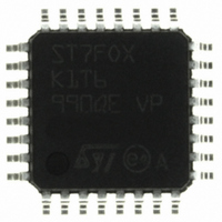
ST7FOXK1T6 STMicroelectronics, ST7FOXK1T6 Datasheet - Page 225

ST7FOXK1T6
Manufacturer Part Number
ST7FOXK1T6
Description
IC MCU 8BIT 1V FLASH MEM 32LQFP
Manufacturer
STMicroelectronics
Series
ST7r
Datasheet
1.ST7FOXF1M6.pdf
(226 pages)
Specifications of ST7FOXK1T6
Core Processor
ST7
Core Size
8-Bit
Speed
8MHz
Connectivity
I²C
Peripherals
LVD, POR, PWM, WDT
Number Of I /o
24
Program Memory Size
4KB (4K x 8)
Program Memory Type
FLASH
Ram Size
384 x 8
Voltage - Supply (vcc/vdd)
4.5 V ~ 5.5 V
Data Converters
A/D 10x10b
Oscillator Type
Internal
Operating Temperature
-40°C ~ 85°C
Package / Case
32-LQFP
Processor Series
ST7FOXx
Core
ST7
Data Bus Width
8 bit
Data Ram Size
384 B
Interface Type
I2C
Maximum Clock Frequency
8 MHz
Number Of Programmable I/os
24
Number Of Timers
4
Maximum Operating Temperature
+ 85 C
Mounting Style
SMD/SMT
Development Tools By Supplier
ST7FLITE-SK/RAIS, STX-RLINK
Minimum Operating Temperature
- 40 C
On-chip Adc
10 bit, 1 Channel
For Use With
497-5049 - KIT STARTER RAISONANCE ST7FLITE
Lead Free Status / RoHS Status
Lead free / RoHS Compliant
Eeprom Size
-
Lead Free Status / Rohs Status
Details
Other names
497-6336
Available stocks
Company
Part Number
Manufacturer
Quantity
Price
Company:
Part Number:
ST7FOXK1T6
Manufacturer:
STMicroelectronics
Quantity:
10 000
Company:
Part Number:
ST7FOXK1T6TR
Manufacturer:
STMicroelectronics
Quantity:
10 000
ST7FOXF1, ST7FOXK1, ST7FOXK2
15
Revision history
Table 102. Document revision history
23-Nov-2007
15-Oct-2007
23-Oct-2007
07-Feb-08
Date
Revision
1
2
3
4
Initial release
Interrupt mapping modified
page
Section 12.8: EMC (electromagnetic compatibility) characteristics on
page 201
Added LVD function
Modified
on page 20
Modified reset configuration for ICCCLK pin
description (32-pin packages) on page 16
Modified
Modified information on eix in
pinout on page 18
Added BREAK2
on page 16
page
Added PB5 in
Modified note on SPI in
Modified
page 90
Modified
page 91
Modified note 4 in
Modified
Modified
Removed bits 2:0 in LTCSR1 register in
register (LTCSR1) on page 115
Modified
Added RCC_CSR in
Added Customized RC calibration section
Modified
references removed from PWM frequency and one pulse mode
paragraphs)
Modified
Modified
Modified
Modified
Added DIP20 package
Added LVD in
Modified
information scheme on page 214
Modified
Modified
59)
82)
Figure 5: ST7FOXF1/ST7FOXK1/ST7FOXK2 memory map
Table 3 on page 19
Figure 44.: Block diagram of input capture mode on
Figure 46.: Long range input capture block diagram on
Figure 6: Typical ICC Interface on page 26
Figure 52: Lite timer 2 block diagram on page 111
Figure 12: Clock management block diagram on page 38
Section 10.2.3: Functional description on page 84
Table 73: On-chip peripheral characteristics on page 193
Section 10.7.1: Introduction on page 173
Section 13.3: Development tools on page 215
Section 13.2: Device ordering information on page 214
Figure 93: ST7FOXF1/ST7FOXK1/ST7FOXK2 ordering
Table 95: Development tool order codes on page 216
Table 101: Thermal characteristics on page 224
modified
and
Figure 1: General block diagram on page 14
Table 3 on page 19
Section 10.2: Dual 12-bit autoreload timer on
(Table 2: Device pin description (32-pin packages)
Section 4.4: ICC interface on page 25
and
Table 4: Hardware register map on page 21
Table 3 on page 19
Table 4: Hardware register map on page 21
(Table 17 on page 58
(added AIN5 on pin n°17)
Changes
Figure 4: 20-pin SO and DIP package
: Lite Timer Control/status
(Table 2: Device pin
and
Revision history
Table 18 on
(32 MHz
225/226


