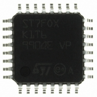
ST7FOXK1T6 STMicroelectronics, ST7FOXK1T6 Datasheet - Page 155

ST7FOXK1T6
Manufacturer Part Number
ST7FOXK1T6
Description
IC MCU 8BIT 1V FLASH MEM 32LQFP
Manufacturer
STMicroelectronics
Series
ST7r
Datasheet
1.ST7FOXF1M6.pdf
(226 pages)
Specifications of ST7FOXK1T6
Core Processor
ST7
Core Size
8-Bit
Speed
8MHz
Connectivity
I²C
Peripherals
LVD, POR, PWM, WDT
Number Of I /o
24
Program Memory Size
4KB (4K x 8)
Program Memory Type
FLASH
Ram Size
384 x 8
Voltage - Supply (vcc/vdd)
4.5 V ~ 5.5 V
Data Converters
A/D 10x10b
Oscillator Type
Internal
Operating Temperature
-40°C ~ 85°C
Package / Case
32-LQFP
Processor Series
ST7FOXx
Core
ST7
Data Bus Width
8 bit
Data Ram Size
384 B
Interface Type
I2C
Maximum Clock Frequency
8 MHz
Number Of Programmable I/os
24
Number Of Timers
4
Maximum Operating Temperature
+ 85 C
Mounting Style
SMD/SMT
Development Tools By Supplier
ST7FLITE-SK/RAIS, STX-RLINK
Minimum Operating Temperature
- 40 C
On-chip Adc
10 bit, 1 Channel
For Use With
497-5049 - KIT STARTER RAISONANCE ST7FLITE
Lead Free Status / RoHS Status
Lead free / RoHS Compliant
Eeprom Size
-
Lead Free Status / Rohs Status
Details
Other names
497-6336
Available stocks
Company
Part Number
Manufacturer
Quantity
Price
Company:
Part Number:
ST7FOXK1T6
Manufacturer:
STMicroelectronics
Quantity:
10 000
Company:
Part Number:
ST7FOXK1T6TR
Manufacturer:
STMicroelectronics
Quantity:
10 000
ST7FOXF1, ST7FOXK1, ST7FOXK2
Note:
Note:
If a Bus Error occurs, a Stop or a repeated Start condition should be generated by the
Master to re-synchronize communication, get the transmission acknowledged and the bus
released for further communication
Bit 0 = GCAL General Call bit (slave mode).
I
Reset value: 0000 0000 (00h)
Bit 7 = FM/SM Fast/Standard I
Bits 6:0 = CC[6:0] 7-bit clock divider bits
The programmed F
I
Reset Value: 0000 0000 (00h)
Bits 7:0 = D[7:0] 8-bit Data register
2
2
C Clock Control register (I2CCCR)
C Data register (I2CDR)
FM/SM
This bit is set by hardware when a general call address is detected on the bus while
ENGC=1. It is cleared by hardware detecting a Stop condition (STOPF=1) or when the
interface is disabled (PE=0).
0: No general call address detected on bus
1: general call address detected on bus
This bit is set and cleared by software. It is not cleared when the interface is disabled
(PE=0).
0: Standard I
1: Fast I
These bits select the speed of the bus (F
cleared when the interface is disabled (PE=0).
Refer to the Electrical Characteristics section for the table of values.
D7
These bits contain the byte to be received or transmitted on the bus.
–
–
7
7
Transmitter mode: byte transmission start automatically when the software writes
in the DR register.
Receiver mode: the first data byte is received automatically in the DR register
using the least significant bit of the address. Then, the following data bytes are
received one by one after reading the DR register.
2
C mode
CC6
D6
2
C mode
SCL
assumes no load on SCL and SDA lines.
CC5
D5
2
C mode bit
CC4
D4
Read / Write
Read / Write
SCL
) depending on the I
CC3
D3
CC2
D2
2
C mode. They are not
On-chip peripherals
CC1
D1
CC0
D0
155/226
0
0


