M30853FJGP#U3 Renesas Electronics America, M30853FJGP#U3 Datasheet - Page 52
M30853FJGP#U3
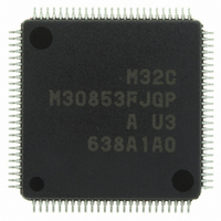
Manufacturer Part Number
M30853FJGP#U3
Description
IC M32C MCU FLASH 100LQFP
Manufacturer
Renesas Electronics America
Series
M16C™ M32C/80r
Datasheets
1.M3087BFLGPU3.pdf
(364 pages)
2.M30853FHFPD5.pdf
(94 pages)
3.M30853FHFPU3.pdf
(544 pages)
Specifications of M30853FJGP#U3
Core Processor
M32C/80
Core Size
16/32-Bit
Speed
32MHz
Connectivity
CAN, I²C, IEBus, SIO, UART/USART
Peripherals
DMA, WDT
Number Of I /o
85
Program Memory Size
512KB (512K x 8)
Program Memory Type
FLASH
Ram Size
24K x 8
Voltage - Supply (vcc/vdd)
3 V ~ 5.5 V
Data Converters
A/D 26x10b; D/A 2x8b
Oscillator Type
Internal
Operating Temperature
-40°C ~ 85°C
Package / Case
100-LQFP
For Use With
R0K330879S001BE - KIT DEV RSK M32C/87R0K330879S000BE - KIT DEV RSK M32C/87
Lead Free Status / RoHS Status
Lead free / RoHS Compliant
Eeprom Size
-
Available stocks
Company
Part Number
Manufacturer
Quantity
Price

Part Number:
M30853FJGP#U3M30853FJGP#D5
Manufacturer:
Renesas Electronics America
Quantity:
10 000


R
R
e
E
v
J
Chapter 2 Addressing Modes
1 .
0
FLG direct
bit,base:11[FB]
bit,base:19[FB]
U
I
O
B
S
Z
D
C
FB relative
9
0 .
B
0
0
3
1
2
9
0
0 -
0
6
1
0 .
0
0
5
3 .
1
p
a
The specified flag is the object to
be operated on.
This addressing can be used in
FCLR and FSET instructions.
The bit that is as much away
from bit 0 at the address indi-
cated by frame base register
(FB) plus the value indicated by
base (added including the sign
bit) as the number of bits indi-
cated by bit is the object to be
operated on.
However, if the address of the
bit to be operated on exceeds
0000000
above bit 25 are ignored and the
address returns to 0000000
0FFFFFF
The address range that can be
specified by bit,base:11 and
bit,base:19 are 128 bytes toward
lower addresses or 127 bytes
toward higher addresses from
the frame base register (FB)
value, and 32,768 bytes toward
lower addresses or 32,767 bytes
toward higher addresses, re-
spectively.
g
e
34
f o
16
16
-0FFFFFF
3
.
3
5
16
, the bits
16
or
If the base value is negative
FB
If the base value is positive
FLG
Register
address
b7
U
base
I
base
2.6 Bit Instruction Addressing
O
Register
address
B
S
Z
Bit position
(Bit position)
Memory
D
b0
C
Related parts for M30853FJGP#U3
Image
Part Number
Description
Manufacturer
Datasheet
Request
R

Part Number:
Description:
KIT STARTER FOR M16C/29
Manufacturer:
Renesas Electronics America
Datasheet:

Part Number:
Description:
KIT STARTER FOR R8C/2D
Manufacturer:
Renesas Electronics America
Datasheet:

Part Number:
Description:
R0K33062P STARTER KIT
Manufacturer:
Renesas Electronics America
Datasheet:

Part Number:
Description:
KIT STARTER FOR R8C/23 E8A
Manufacturer:
Renesas Electronics America
Datasheet:

Part Number:
Description:
KIT STARTER FOR R8C/25
Manufacturer:
Renesas Electronics America
Datasheet:

Part Number:
Description:
KIT STARTER H8S2456 SHARPE DSPLY
Manufacturer:
Renesas Electronics America
Datasheet:

Part Number:
Description:
KIT STARTER FOR R8C38C
Manufacturer:
Renesas Electronics America
Datasheet:

Part Number:
Description:
KIT STARTER FOR R8C35C
Manufacturer:
Renesas Electronics America
Datasheet:

Part Number:
Description:
KIT STARTER FOR R8CL3AC+LCD APPS
Manufacturer:
Renesas Electronics America
Datasheet:
Part Number:
Description:
KIT STARTER FOR RX610
Manufacturer:
Renesas Electronics America
Datasheet:

Part Number:
Description:
KIT STARTER FOR R32C/118
Manufacturer:
Renesas Electronics America
Datasheet:

Part Number:
Description:
KIT DEV RSK-R8C/26-29
Manufacturer:
Renesas Electronics America
Datasheet:

Part Number:
Description:
KIT STARTER FOR SH7124
Manufacturer:
Renesas Electronics America
Datasheet:

Part Number:
Description:
KIT STARTER FOR H8SX/1622
Manufacturer:
Renesas Electronics America
Datasheet:

Part Number:
Description:
KIT DEV FOR SH7203
Manufacturer:
Renesas Electronics America
Datasheet: