M30853FJGP#U3 Renesas Electronics America, M30853FJGP#U3 Datasheet - Page 25
M30853FJGP#U3
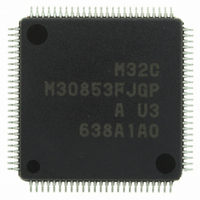
Manufacturer Part Number
M30853FJGP#U3
Description
IC M32C MCU FLASH 100LQFP
Manufacturer
Renesas Electronics America
Series
M16C™ M32C/80r
Datasheets
1.M3087BFLGPU3.pdf
(364 pages)
2.M30853FHFPD5.pdf
(94 pages)
3.M30853FHFPU3.pdf
(544 pages)
Specifications of M30853FJGP#U3
Core Processor
M32C/80
Core Size
16/32-Bit
Speed
32MHz
Connectivity
CAN, I²C, IEBus, SIO, UART/USART
Peripherals
DMA, WDT
Number Of I /o
85
Program Memory Size
512KB (512K x 8)
Program Memory Type
FLASH
Ram Size
24K x 8
Voltage - Supply (vcc/vdd)
3 V ~ 5.5 V
Data Converters
A/D 26x10b; D/A 2x8b
Oscillator Type
Internal
Operating Temperature
-40°C ~ 85°C
Package / Case
100-LQFP
For Use With
R0K330879S001BE - KIT DEV RSK M32C/87R0K330879S000BE - KIT DEV RSK M32C/87
Lead Free Status / RoHS Status
Lead free / RoHS Compliant
Eeprom Size
-
Available stocks
Company
Part Number
Manufacturer
Quantity
Price

Part Number:
M30853FJGP#U3M30853FJGP#D5
Manufacturer:
Renesas Electronics America
Quantity:
10 000


R
R
1.4 Flag Register (FLG)
e
E
v
J
Chapter 1 Overview
Figure 1.4.1 shows a configuration of the flag register (FLG). The function of each flag is detailed below.
1 .
0
(1) Bit 0: Carry Flag (C flag)
(2) Bit 1: Debug Flag (D flag)
(3) Bit 2: Zero Flag (Z flag)
(4) Bit 3: Sign Flag (S flag)
(5) Bit 4: Register Bank Select Flag (B flag)
(6) Bit 5: Overflow Flag (O flag)
(7) Bit 6: Interrupt Enable Flag (I flag)
(8) Bit 7: Stack Pointer Select Flag (U flag)
(9) Bits 8-11: Reserved Area
9
0 .
B
This flag holds a carry, borrow, or shifted-out bit that has occurred in the arithmetic/logic unit.
This flag enables a single-step interrupt.
When this flag is set (= 1), a single-step interrupt is generated after an instruction is executed. When
an interrupt is acknowledged, this flag is cleared to 0.
This flag is set when an arithmetic operation resulted in 0; otherwise, this flag is 0.
This flag is set when an arithmetic operation resulted in a negative value; otherwise, this flag is 0.
This flag selects a register bank. If this flag is 0, register bank 0 is selected; when the flag is 1,
register bank 1 is selected.
This flag is set when an arithmetic operation resulted in overflow.
This flag enables a maskable interrupt.
When this flag is 0, the interrupt is disabled; when the flag is 1, the interrupt is enabled. When the
interrupt is acknowledged, this flag is cleared to 0.
When this flag is 0, the interrupt stack pointer (ISP) is selected; when the flag is 1, the user stack
pointer (USP) is selected.
This flag is cleared to 0 when a hardware interrupt is acknowledged or the INT instruction of software
interrupt numbers 0 to 31 is executed.
0
0
3
1
2
9
0
0 -
0
6
1
0 .
0
0
5
3 .
1
p
a
g
e
7
f o
3
3
5
1.4 Flag Register (FLG)
Related parts for M30853FJGP#U3
Image
Part Number
Description
Manufacturer
Datasheet
Request
R

Part Number:
Description:
KIT STARTER FOR M16C/29
Manufacturer:
Renesas Electronics America
Datasheet:

Part Number:
Description:
KIT STARTER FOR R8C/2D
Manufacturer:
Renesas Electronics America
Datasheet:

Part Number:
Description:
R0K33062P STARTER KIT
Manufacturer:
Renesas Electronics America
Datasheet:

Part Number:
Description:
KIT STARTER FOR R8C/23 E8A
Manufacturer:
Renesas Electronics America
Datasheet:

Part Number:
Description:
KIT STARTER FOR R8C/25
Manufacturer:
Renesas Electronics America
Datasheet:

Part Number:
Description:
KIT STARTER H8S2456 SHARPE DSPLY
Manufacturer:
Renesas Electronics America
Datasheet:

Part Number:
Description:
KIT STARTER FOR R8C38C
Manufacturer:
Renesas Electronics America
Datasheet:

Part Number:
Description:
KIT STARTER FOR R8C35C
Manufacturer:
Renesas Electronics America
Datasheet:

Part Number:
Description:
KIT STARTER FOR R8CL3AC+LCD APPS
Manufacturer:
Renesas Electronics America
Datasheet:
Part Number:
Description:
KIT STARTER FOR RX610
Manufacturer:
Renesas Electronics America
Datasheet:

Part Number:
Description:
KIT STARTER FOR R32C/118
Manufacturer:
Renesas Electronics America
Datasheet:

Part Number:
Description:
KIT DEV RSK-R8C/26-29
Manufacturer:
Renesas Electronics America
Datasheet:

Part Number:
Description:
KIT STARTER FOR SH7124
Manufacturer:
Renesas Electronics America
Datasheet:

Part Number:
Description:
KIT STARTER FOR H8SX/1622
Manufacturer:
Renesas Electronics America
Datasheet:

Part Number:
Description:
KIT DEV FOR SH7203
Manufacturer:
Renesas Electronics America
Datasheet: