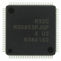
M30853FJGP#U3 Renesas Electronics America, M30853FJGP#U3 Datasheet - Page 343

M30853FJGP#U3
Manufacturer Part Number
M30853FJGP#U3
Description
IC M32C MCU FLASH 100LQFP
Manufacturer
Renesas Electronics America
Series
M16C™ M32C/80r
Datasheets
1.M3087BFLGPU3.pdf
(364 pages)
2.M30853FHFPD5.pdf
(94 pages)
3.M30853FHFPU3.pdf
(544 pages)
Specifications of M30853FJGP#U3
Core Processor
M32C/80
Core Size
16/32-Bit
Speed
32MHz
Connectivity
CAN, I²C, IEBus, SIO, UART/USART
Peripherals
DMA, WDT
Number Of I /o
85
Program Memory Size
512KB (512K x 8)
Program Memory Type
FLASH
Ram Size
24K x 8
Voltage - Supply (vcc/vdd)
3 V ~ 5.5 V
Data Converters
A/D 26x10b; D/A 2x8b
Oscillator Type
Internal
Operating Temperature
-40°C ~ 85°C
Package / Case
100-LQFP
For Use With
R0K330879S001BE - KIT DEV RSK M32C/87R0K330879S000BE - KIT DEV RSK M32C/87
Lead Free Status / RoHS Status
Lead free / RoHS Compliant
Eeprom Size
-
Available stocks
Company
Part Number
Manufacturer
Quantity
Price
Part Number:
M30853FJGP#U3M30853FJGP#D5
Manufacturer:
Renesas Electronics America
Quantity:
10 000
- Current page: 343 of 364
- Download datasheet (3Mb)
R
R
e
E
v
J
Chapter 6
Figure 6.1.3. When executing an instruction to read from even addresses starting from an even address
1 .
0
9
0 .
B
0
0
3
1
Instructions
under execution
Data bus (L)
Fetch code
Address bus
Data bus (H)
2
BCLK
Instruction
queue buffer
RD
9
WR
0
0 -
0
Content at jump
address is prefetched at
the same time the
instruction queue buffer
is cleared.
6
1
Sample program
Address
FFC024
FFC024
FFC025
FFC026
FFC027
FFC028
FFC029
FFC02A
FFC02B
FFC02C
FFC02C
FFC030
FFC031
FFC032
FFC033
FFC034
FFC035
FFC036
FFC037
FFC038
0 .
0
0
5
3 .
(Program area: 16-bit bus without wait state; Data area: 16-bit bus without wait state)
Calculation number of cycles
1
DR : Indicates a data read.
p
P : Indicates a prefetch (reading from memory into the instruction queue buffer).
a
Jump address
g
: Indicates the locations of the instruction queue buffer that are cleared.
e
FFC02A FFC02C FFC02E FFC030
Code
7A
DE
DE
DE
DE
DE
DE
DE
325
7A
DE
DE
DE
DE
DE
DE
DE
B9FB0020
7A
DE
DE
DE
DE
DE
DE
DE
TEST_10:
TEST_11:
TEST_12:
JMP TEST_11
DE
DE
P
f o
B9
FB
3
3
P
5
FB
B9
Instruction
JMP
NOP
NOP
NOP
NOP
NOP
NOP
NOP
MOV.W:G
JMP
NOP
NOP
NOP
NOP
NOP
NOP
NOP
FB
B9
00
20
P
20
00
Fetch
B9FB
DE
7A
00
20
DE
7A
P
02000h,R1
TEST_11
TEST_12
Fetch
MOV.W
02000
0020
DE
7A
DR
AA
AA
FFC032 FFC034 FFC038 FFC03A
DE
DE
DE
7A
Content at address 2001
Content at address 2000
DE
DE
P
Fetch
7A
DE
DE
DE
DE
DE
JMP TEST_12
DE
DE
P
FB
B9
P
FB
B9
6.1 Instruction queue buffer
Content at jump address
is prefetched at the
same time the instruction
queue buffer is cleared.
16
16
B9
FB
00
20
P
20
00
Related parts for M30853FJGP#U3
Image
Part Number
Description
Manufacturer
Datasheet
Request
R

Part Number:
Description:
KIT STARTER FOR M16C/29
Manufacturer:
Renesas Electronics America
Datasheet:

Part Number:
Description:
KIT STARTER FOR R8C/2D
Manufacturer:
Renesas Electronics America
Datasheet:

Part Number:
Description:
R0K33062P STARTER KIT
Manufacturer:
Renesas Electronics America
Datasheet:

Part Number:
Description:
KIT STARTER FOR R8C/23 E8A
Manufacturer:
Renesas Electronics America
Datasheet:

Part Number:
Description:
KIT STARTER FOR R8C/25
Manufacturer:
Renesas Electronics America
Datasheet:

Part Number:
Description:
KIT STARTER H8S2456 SHARPE DSPLY
Manufacturer:
Renesas Electronics America
Datasheet:

Part Number:
Description:
KIT STARTER FOR R8C38C
Manufacturer:
Renesas Electronics America
Datasheet:

Part Number:
Description:
KIT STARTER FOR R8C35C
Manufacturer:
Renesas Electronics America
Datasheet:

Part Number:
Description:
KIT STARTER FOR R8CL3AC+LCD APPS
Manufacturer:
Renesas Electronics America
Datasheet:

Part Number:
Description:
KIT STARTER FOR RX610
Manufacturer:
Renesas Electronics America
Datasheet:

Part Number:
Description:
KIT STARTER FOR R32C/118
Manufacturer:
Renesas Electronics America
Datasheet:

Part Number:
Description:
KIT DEV RSK-R8C/26-29
Manufacturer:
Renesas Electronics America
Datasheet:

Part Number:
Description:
KIT STARTER FOR SH7124
Manufacturer:
Renesas Electronics America
Datasheet:

Part Number:
Description:
KIT STARTER FOR H8SX/1622
Manufacturer:
Renesas Electronics America
Datasheet:

Part Number:
Description:
KIT DEV FOR SH7203
Manufacturer:
Renesas Electronics America
Datasheet:


