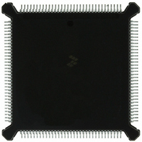
MC68332GCEH16 Freescale Semiconductor, MC68332GCEH16 Datasheet - Page 95

MC68332GCEH16
Manufacturer Part Number
MC68332GCEH16
Description
IC MCU 32BIT 16MHZ 132-PQFP
Manufacturer
Freescale Semiconductor
Series
M683xxr
Specifications of MC68332GCEH16
Core Processor
CPU32
Core Size
32-Bit
Speed
16MHz
Connectivity
EBI/EMI, SCI, SPI, UART/USART
Peripherals
POR, PWM, WDT
Number Of I /o
15
Program Memory Type
ROMless
Ram Size
2K x 8
Voltage - Supply (vcc/vdd)
4.5 V ~ 5.5 V
Oscillator Type
Internal
Operating Temperature
-40°C ~ 85°C
Package / Case
132-QFP
Cpu Family
68K/M683xx
Device Core
ColdFire
Device Core Size
32b
Frequency (max)
16MHz
Interface Type
QSPI/SCI/UART
Program Memory Size
Not Required
Total Internal Ram Size
2KB
# I/os (max)
15
Number Of Timers - General Purpose
16
Operating Supply Voltage (typ)
5V
Operating Supply Voltage (max)
5.5V
Operating Supply Voltage (min)
4.5V
Instruction Set Architecture
RISC
Operating Temp Range
-40C to 85C
Operating Temperature Classification
Industrial
Mounting
Surface Mount
Pin Count
132
Package Type
PQFP
Controller Family/series
68K
No. Of I/o's
15
Ram Memory Size
2KB
Cpu Speed
16MHz
No. Of Timers
16
Embedded Interface Type
QSPI, SCI, UART
Digital Ic Case Style
PQFP
Rohs Compliant
Yes
Processor Series
M683xx
Core
CPU32
Data Bus Width
32 bit
Data Ram Size
2 KB
Maximum Clock Frequency
16 MHz
Number Of Programmable I/os
15
Number Of Timers
16
Maximum Operating Temperature
+ 85 C
Mounting Style
SMD/SMT
Minimum Operating Temperature
- 40 C
Lead Free Status / RoHS Status
Lead free / RoHS Compliant
Eeprom Size
-
Program Memory Size
-
Data Converters
-
Lead Free Status / Rohs Status
Compliant
Available stocks
Company
Part Number
Manufacturer
Quantity
Price
Company:
Part Number:
MC68332GCEH16
Manufacturer:
Freescale Semiconductor
Quantity:
10 000
4.8.1.4 PORTC Data Register
4.8.2 Chip-Select Operation
4.8.3 Using Chip-Select Signals for Interrupt Acknowledge
MC68332
USER’S MANUAL
to %00 (CPU space), interrupt priority (ADDR[3:1]) is compared to IPL value. If the val-
ues are the same, and other option register constraints are satisfied, a chip select sig-
nal is asserted. This field only affects the response of chip selects and does not affect
interrupt recognition by the CPU. Encoding %000 causes a chip-select signal to be as-
serted regardless of interrupt acknowledge cycle priority, provided all other constraints
are met.
The AVEC bit selects one of two methods of acquiring an interrupt vector during an
external interrupt acknowledge cycle. The internal autovector signal is generated only
in response to interrupt requests from the SIM IRQ pins.
The PORTC data register latches data for PORTC pins programmed as discrete out-
puts. When a pin is assigned as a discrete output, the value in this register appears at
the output. PC[6:0] correspond to CS[9:3]. Bit 7 is not used. Writing to this bit has no
effect, and it always reads zero.
When the MCU makes an access, enabled chip-select circuits compare the following
items:
When a match occurs, the chip-select signal is asserted. Assertion occurs at the same
time as AS or DS assertion in asynchronous mode. Assertion is synchronized with
ECLK in synchronous mode. In asynchronous mode, the value of the DSACK field de-
termines whether DSACK is generated internally.DSACK also determines the number
of wait states inserted before internal DSACK assertion.
The speed of an external device determines whether internal wait states are needed.
Normally, wait states are inserted into the bus cycle during S3 until a peripheral as-
serts DSACK. If a peripheral does not generate DSACK, internal DSACK generation
must be selected and a predetermined number of wait states can be programmed into
the chip-select option register.
Refer to the SIM Reference Manual (SIMRM/AD) for further information.
Ordinary I/O bus cycles use supervisor space access, but interrupt acknowledge bus
cycles use CPU space access. Refer to 4.5.4 CPU Space Cycles and 4.7 Interrupts
for more information. There are no differences in flow for chip selects in each type of
space, but base and option registers must be properly programmed for each type of
external bus cycle.
1. Function codes to SPACE fields, and to the IPL field if the SPACE field encod-
2. Appropriate ADDR bits to base address fields.
3. Read/write status to R/W fields.
4. ADDR0 and/or SIZ bits to the BYTE field (16-bit ports only).
5. Priority of the interrupt being acknowledged (ADDR[3:1]) to IPL fields (when the
ing is not for CPU32 space.
access is an interrupt acknowledge cycle).
Freescale Semiconductor, Inc.
For More Information On This Product,
SYSTEM INTEGRATION MODULE
Go to: www.freescale.com
4-55


