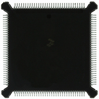
MC68332GCEH16 Freescale Semiconductor, MC68332GCEH16 Datasheet - Page 91

MC68332GCEH16
Manufacturer Part Number
MC68332GCEH16
Description
IC MCU 32BIT 16MHZ 132-PQFP
Manufacturer
Freescale Semiconductor
Series
M683xxr
Specifications of MC68332GCEH16
Core Processor
CPU32
Core Size
32-Bit
Speed
16MHz
Connectivity
EBI/EMI, SCI, SPI, UART/USART
Peripherals
POR, PWM, WDT
Number Of I /o
15
Program Memory Type
ROMless
Ram Size
2K x 8
Voltage - Supply (vcc/vdd)
4.5 V ~ 5.5 V
Oscillator Type
Internal
Operating Temperature
-40°C ~ 85°C
Package / Case
132-QFP
Cpu Family
68K/M683xx
Device Core
ColdFire
Device Core Size
32b
Frequency (max)
16MHz
Interface Type
QSPI/SCI/UART
Program Memory Size
Not Required
Total Internal Ram Size
2KB
# I/os (max)
15
Number Of Timers - General Purpose
16
Operating Supply Voltage (typ)
5V
Operating Supply Voltage (max)
5.5V
Operating Supply Voltage (min)
4.5V
Instruction Set Architecture
RISC
Operating Temp Range
-40C to 85C
Operating Temperature Classification
Industrial
Mounting
Surface Mount
Pin Count
132
Package Type
PQFP
Controller Family/series
68K
No. Of I/o's
15
Ram Memory Size
2KB
Cpu Speed
16MHz
No. Of Timers
16
Embedded Interface Type
QSPI, SCI, UART
Digital Ic Case Style
PQFP
Rohs Compliant
Yes
Processor Series
M683xx
Core
CPU32
Data Bus Width
32 bit
Data Ram Size
2 KB
Maximum Clock Frequency
16 MHz
Number Of Programmable I/os
15
Number Of Timers
16
Maximum Operating Temperature
+ 85 C
Mounting Style
SMD/SMT
Minimum Operating Temperature
- 40 C
Lead Free Status / RoHS Status
Lead free / RoHS Compliant
Eeprom Size
-
Program Memory Size
-
Data Converters
-
Lead Free Status / Rohs Status
Compliant
Available stocks
Company
Part Number
Manufacturer
Quantity
Price
Company:
Part Number:
MC68332GCEH16
Manufacturer:
Freescale Semiconductor
Quantity:
10 000
- Current page: 91 of 265
- Download datasheet (7Mb)
4.8.1 Chip-Select Registers
MC68332
USER’S MANUAL
in the corresponding option register is programmed to a nonzero value, selecting a
transfer size. The chip-select option must not be written until a base address has been
written to a proper base address register. CSBOOT is automatically asserted out of
reset. Alternate functions for chip-select pins are enabled if appropriate data bus pins
are held low at the release of the reset signal (refer to 4.6.3.1 Data Bus Mode Selec-
tion for more information). Figure 4-18 is a functional diagram of a single chip-select
circuit.
Each chip-select pin can have one or more functions. Chip-select pin assignment reg-
isters (CSPAR[0:1]) determine functions of the pins. Pin assignment registers also de-
termine port size (8- or 16-bit) for dynamic bus allocation. A pin data register (PORTC)
latches data for chip-select pins that are used for discrete output.
Blocks of addresses are assigned to each chip-select function. Block sizes of two
Kbytes to one Mbyte can be selected by writing values to the appropriate base address
register (CSBAR[0:10], CSBARBT). Address blocks for separate chip-select functions
can overlap.
Chip select option registers (CSOR[0:10], CSORBT) determine timing of and condi-
tions for assertion of chip-select signals. Eight parameters, including operating mode,
access size, synchronization, and wait state insertion can be specified.
Initialization software usually resides in a peripheral memory device controlled by the
chip-select circuits. A set of special chip-select functions and registers (CSORBT, CS-
BARBT) is provided to support bootstrap operation.
Comprehensive address maps and register diagrams are provided in APPENDIX D
REGISTER SUMMARY.
BUS CONTROL
DSACK
AVEC
INTERNAL
ADDRESS
SIGNALS
Figure 4-18 Chip-Select Circuit Block Diagram
GENERATOR
AVEC
Freescale Semiconductor, Inc.
For More Information On This Product,
BASE ADDRESS REGISTER
ADDRESS COMPARATOR
OPTION REGISTER
OPTION COMPARE
SYSTEM INTEGRATION MODULE
Go to: www.freescale.com
GENERATOR
DSACK
ASSIGNMENT
REGISTER
PIN
CONTROL
TIMING
AND
REGISTER
DATA
PIN
PIN
CHIP SEL BLOCK
4-51
Related parts for MC68332GCEH16
Image
Part Number
Description
Manufacturer
Datasheet
Request
R
Part Number:
Description:
Manufacturer:
Freescale Semiconductor, Inc
Datasheet:
Part Number:
Description:
Manufacturer:
Freescale Semiconductor, Inc
Datasheet:
Part Number:
Description:
Manufacturer:
Freescale Semiconductor, Inc
Datasheet:
Part Number:
Description:
Manufacturer:
Freescale Semiconductor, Inc
Datasheet:
Part Number:
Description:
Manufacturer:
Freescale Semiconductor, Inc
Datasheet:
Part Number:
Description:
Manufacturer:
Freescale Semiconductor, Inc
Datasheet:
Part Number:
Description:
Manufacturer:
Freescale Semiconductor, Inc
Datasheet:
Part Number:
Description:
Manufacturer:
Freescale Semiconductor, Inc
Datasheet:
Part Number:
Description:
Manufacturer:
Freescale Semiconductor, Inc
Datasheet:
Part Number:
Description:
Manufacturer:
Freescale Semiconductor, Inc
Datasheet:
Part Number:
Description:
Manufacturer:
Freescale Semiconductor, Inc
Datasheet:
Part Number:
Description:
Manufacturer:
Freescale Semiconductor, Inc
Datasheet:
Part Number:
Description:
Manufacturer:
Freescale Semiconductor, Inc
Datasheet:
Part Number:
Description:
Manufacturer:
Freescale Semiconductor, Inc
Datasheet:
Part Number:
Description:
Manufacturer:
Freescale Semiconductor, Inc
Datasheet:


