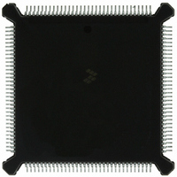
MC68332GCEH16 Freescale Semiconductor, MC68332GCEH16 Datasheet - Page 61

MC68332GCEH16
Manufacturer Part Number
MC68332GCEH16
Description
IC MCU 32BIT 16MHZ 132-PQFP
Manufacturer
Freescale Semiconductor
Series
M683xxr
Specifications of MC68332GCEH16
Core Processor
CPU32
Core Size
32-Bit
Speed
16MHz
Connectivity
EBI/EMI, SCI, SPI, UART/USART
Peripherals
POR, PWM, WDT
Number Of I /o
15
Program Memory Type
ROMless
Ram Size
2K x 8
Voltage - Supply (vcc/vdd)
4.5 V ~ 5.5 V
Oscillator Type
Internal
Operating Temperature
-40°C ~ 85°C
Package / Case
132-QFP
Cpu Family
68K/M683xx
Device Core
ColdFire
Device Core Size
32b
Frequency (max)
16MHz
Interface Type
QSPI/SCI/UART
Program Memory Size
Not Required
Total Internal Ram Size
2KB
# I/os (max)
15
Number Of Timers - General Purpose
16
Operating Supply Voltage (typ)
5V
Operating Supply Voltage (max)
5.5V
Operating Supply Voltage (min)
4.5V
Instruction Set Architecture
RISC
Operating Temp Range
-40C to 85C
Operating Temperature Classification
Industrial
Mounting
Surface Mount
Pin Count
132
Package Type
PQFP
Controller Family/series
68K
No. Of I/o's
15
Ram Memory Size
2KB
Cpu Speed
16MHz
No. Of Timers
16
Embedded Interface Type
QSPI, SCI, UART
Digital Ic Case Style
PQFP
Rohs Compliant
Yes
Processor Series
M683xx
Core
CPU32
Data Bus Width
32 bit
Data Ram Size
2 KB
Maximum Clock Frequency
16 MHz
Number Of Programmable I/os
15
Number Of Timers
16
Maximum Operating Temperature
+ 85 C
Mounting Style
SMD/SMT
Minimum Operating Temperature
- 40 C
Lead Free Status / RoHS Status
Lead free / RoHS Compliant
Eeprom Size
-
Program Memory Size
-
Data Converters
-
Lead Free Status / Rohs Status
Compliant
Available stocks
Company
Part Number
Manufacturer
Quantity
Price
Company:
Part Number:
MC68332GCEH16
Manufacturer:
Freescale Semiconductor
Quantity:
10 000
- Current page: 61 of 265
- Download datasheet (7Mb)
4.4.3 Operand Alignment
MC68332
USER’S MANUAL
If the CPU is executing an instruction that reads a long-word operand from a 16-bit
port, the MCU latches the 16 bits of valid data and then runs another bus cycle to ob-
tain the other 16 bits. The operation for an 8-bit port is similar, but requires four read
cycles. The addressed device uses the DSACK signals to indicate the port width. For
instance, a 16-bit device always returns DSACK for a 16-bit port (regardless of wheth-
er the bus cycle is a byte or word operation).
Dynamic bus sizing requires that the portion of the data bus used for a transfer to or
from a particular port size be fixed. A 16-bit port must reside on data bus bits [15:0],
and an 8-bit port must reside on data bus bits [15:8]. This minimizes the number of bus
cycles needed to transfer data and ensures that the MCU transfers valid data.
The MCU always attempts to transfer the maximum amount of data on all bus cycles.
For a word operation, it is assumed that the port is 16 bits wide when the bus cycle
begins.
Operand bytes are designated as shown in Figure 4-8. OP[0:3] represent the order of
access. For instance, OP0 is the most significant byte of a long-word operand, and is
accessed first, while OP3, the least significant byte, is accessed last. The two bytes of
a word-length operand are OP0 (most significant) and OP1. The single byte of a byte-
length operand is OP0.
The EBI data multiplexer establishes the necessary connections for different combi-
nations of address and data sizes. The multiplexer takes the two bytes of the 16-bit
bus and routes them to their required positions. Positioning of bytes is determined by
the size and address outputs. SIZ1 and SIZ0 indicate the remaining number of bytes
to be transferred during the current bus cycle. The number of bytes transferred is equal
to or less than the size indicated by SIZ1 and SIZ0, depending on port width.
ADDR0 also affects the operation of the data multiplexer. During an operand transfer,
ADDR[23:1] indicate the word base address of the portion of the operand to be ac-
cessed, and ADDR0 indicates the byte offset from the base.
DSACK1
1
1
0
0
Long Word
Three Byte
Operand
Word
Byte
Freescale Semiconductor, Inc.
Table 4-12 Effect of DSACK Signals
DSACK0
For More Information On This Product,
Figure 4-8 Operand Byte Order
1
0
1
0
SYSTEM INTEGRATION MODULE
31
Go to: www.freescale.com
OP0
Insert Wait States in Current Bus Cycle
Complete Cycle — Data Bus Port Size is 8 Bits
Complete Cycle — Data Bus Port Size is 16 Bits
Reserved
24
23
OP1
OP0
Byte Order
16
15
Result
OP2
OP1
OP0
8
7
OP3
OP2
OP1
OP0
0
4-21
Related parts for MC68332GCEH16
Image
Part Number
Description
Manufacturer
Datasheet
Request
R
Part Number:
Description:
Manufacturer:
Freescale Semiconductor, Inc
Datasheet:
Part Number:
Description:
Manufacturer:
Freescale Semiconductor, Inc
Datasheet:
Part Number:
Description:
Manufacturer:
Freescale Semiconductor, Inc
Datasheet:
Part Number:
Description:
Manufacturer:
Freescale Semiconductor, Inc
Datasheet:
Part Number:
Description:
Manufacturer:
Freescale Semiconductor, Inc
Datasheet:
Part Number:
Description:
Manufacturer:
Freescale Semiconductor, Inc
Datasheet:
Part Number:
Description:
Manufacturer:
Freescale Semiconductor, Inc
Datasheet:
Part Number:
Description:
Manufacturer:
Freescale Semiconductor, Inc
Datasheet:
Part Number:
Description:
Manufacturer:
Freescale Semiconductor, Inc
Datasheet:
Part Number:
Description:
Manufacturer:
Freescale Semiconductor, Inc
Datasheet:
Part Number:
Description:
Manufacturer:
Freescale Semiconductor, Inc
Datasheet:
Part Number:
Description:
Manufacturer:
Freescale Semiconductor, Inc
Datasheet:
Part Number:
Description:
Manufacturer:
Freescale Semiconductor, Inc
Datasheet:
Part Number:
Description:
Manufacturer:
Freescale Semiconductor, Inc
Datasheet:
Part Number:
Description:
Manufacturer:
Freescale Semiconductor, Inc
Datasheet:


