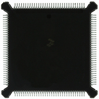
MC68332GCEH16 Freescale Semiconductor, MC68332GCEH16 Datasheet - Page 149

MC68332GCEH16
Manufacturer Part Number
MC68332GCEH16
Description
IC MCU 32BIT 16MHZ 132-PQFP
Manufacturer
Freescale Semiconductor
Series
M683xxr
Specifications of MC68332GCEH16
Core Processor
CPU32
Core Size
32-Bit
Speed
16MHz
Connectivity
EBI/EMI, SCI, SPI, UART/USART
Peripherals
POR, PWM, WDT
Number Of I /o
15
Program Memory Type
ROMless
Ram Size
2K x 8
Voltage - Supply (vcc/vdd)
4.5 V ~ 5.5 V
Oscillator Type
Internal
Operating Temperature
-40°C ~ 85°C
Package / Case
132-QFP
Cpu Family
68K/M683xx
Device Core
ColdFire
Device Core Size
32b
Frequency (max)
16MHz
Interface Type
QSPI/SCI/UART
Program Memory Size
Not Required
Total Internal Ram Size
2KB
# I/os (max)
15
Number Of Timers - General Purpose
16
Operating Supply Voltage (typ)
5V
Operating Supply Voltage (max)
5.5V
Operating Supply Voltage (min)
4.5V
Instruction Set Architecture
RISC
Operating Temp Range
-40C to 85C
Operating Temperature Classification
Industrial
Mounting
Surface Mount
Pin Count
132
Package Type
PQFP
Controller Family/series
68K
No. Of I/o's
15
Ram Memory Size
2KB
Cpu Speed
16MHz
No. Of Timers
16
Embedded Interface Type
QSPI, SCI, UART
Digital Ic Case Style
PQFP
Rohs Compliant
Yes
Processor Series
M683xx
Core
CPU32
Data Bus Width
32 bit
Data Ram Size
2 KB
Maximum Clock Frequency
16 MHz
Number Of Programmable I/os
15
Number Of Timers
16
Maximum Operating Temperature
+ 85 C
Mounting Style
SMD/SMT
Minimum Operating Temperature
- 40 C
Lead Free Status / RoHS Status
Lead free / RoHS Compliant
Eeprom Size
-
Program Memory Size
-
Data Converters
-
Lead Free Status / Rohs Status
Compliant
Available stocks
Company
Part Number
Manufacturer
Quantity
Price
Company:
Part Number:
MC68332GCEH16
Manufacturer:
Freescale Semiconductor
Quantity:
10 000
6.4.3.4 Parity Checking
6.4.3.5 Transmitter Operation
MC68332
USER’S MANUAL
time (RT) sampling clock with a frequency 16 times that of the SCI baud clock. The
SCI determines the position of bit boundaries from transitions within the received
waveform, and adjusts sampling points to the proper positions within the bit period.
The parity type (PT) bit in SCCR1 selects either even (PT = 0) or odd (PT = 1) parity.
PT affects received and transmitted data. The parity enable (PE) bit in SCCR1 deter-
mines whether parity checking is enabled (PE = 1) or disabled (PE = 0). When PE is
set, the MSB of the data in a frame is used for the parity function. For transmitted data,
a parity bit is generated; for received data, the parity bit is checked. When parity check-
ing is enabled, the parity flag (PF) in the SCI status register (SCSR) is set if a parity
error is detected.
Enabling parity affects the number of data bits in a frame, which can in turn affect
frame size. Table 6-6 shows possible data and parity formats.
The transmitter consists of a serial shifter and a parallel data register (TDR) located in
the SCI data register (SCDR). The serial shifter cannot be directly accessed by the
CPU. The transmitter is double-buffered, which means that data can be loaded into
the TDR while other data is shifted out. The transmitter enable (TE) bit in SCCR1 en-
ables (TE = 1) and disables (TE = 0) the transmitter.
Shifter output is connected to the TXD pin while the transmitter is operating (TE = 1,
or TE = 0 and transmission in progress). Wired-OR operation should be specified
when more than one transmitter is used on the same SCI bus. The wired-OR mode
select bit (WOMS) in SCCR1 determines whether TXD is an open-drain (wired-OR)
output or a normal CMOS output. An external pull-up resistor on the TXD pin is nec-
essary for wired-OR operation. WOMS controls TXD function whether the pin is used
for SCI transmissions (TE = 1) or as a general-purpose I/O pin.
Data to be transmitted is written to TDR, then transferred to the serial shifter. The
transmit data register empty (TDRE) flag in SCSR shows the status of TDR. When
TDRE = 0, TDR contains data that has not been transferred to the shifter. Writing to
TDR again overwrites the data. TDRE is set when the data in TDR is transferred to the
shifter. Before new data can be written to TDR, however, the processor must clear
TDRE by writing to SCSR. If new data is written to TDR without first clearing TDRE,
the data will not be transmitted.
Table 6-6 Effect of Parity Checking on Data Size
Freescale Semiconductor, Inc.
M
0
0
1
1
For More Information On This Product,
PE
0
1
0
1
QUEUED SERIAL MODULE
Go to: www.freescale.com
7 Data Bits, 1 Parity Bit
8 Data Bits, 1 Parity Bit
8 Data Bits
9 Data Bits
Result
6-27


