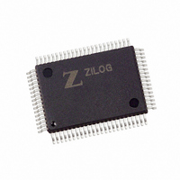
Z16F6411FI20SG Zilog, Z16F6411FI20SG Datasheet - Page 323

Z16F6411FI20SG
Manufacturer Part Number
Z16F6411FI20SG
Description
IC ZNEO MCU FLASH 64K 80QFP
Manufacturer
Zilog
Series
Encore!® ZNEOr
Datasheet
1.Z16F2800100ZCOG.pdf
(388 pages)
Specifications of Z16F6411FI20SG
Core Processor
ZNEO
Core Size
16-Bit
Speed
20MHz
Connectivity
EBI/EMI, I²C, IrDA, LIN, SPI, UART/USART
Peripherals
Brown-out Detect/Reset, DMA, POR, PWM, WDT
Number Of I /o
60
Program Memory Size
64KB (64K x 8)
Program Memory Type
FLASH
Ram Size
4K x 8
Voltage - Supply (vcc/vdd)
2.7 V ~ 3.6 V
Data Converters
A/D 12x10b
Oscillator Type
Internal
Operating Temperature
0°C ~ 70°C
Package / Case
80-BQFP
Processor Series
Z16F6x
Core
Zneo
Data Bus Width
16 bit
Data Ram Size
4 B
Interface Type
ESPI, I2C, UART
Maximum Clock Frequency
20 MHz
Number Of Programmable I/os
60
Number Of Timers
4
Operating Supply Voltage
2.7 V to 3.6 V
Maximum Operating Temperature
+ 70 C
Mounting Style
SMD/SMT
Development Tools By Supplier
Z16F2800100ZCOG
Minimum Operating Temperature
0 C
On-chip Adc
10 bit, 12 Channel
For Use With
770-1003 - ISP 4PORT FOR ZILOG ZNEO MCU269-4537 - DEV KIT FOR Z16F ZNEO
Lead Free Status / RoHS Status
Lead free / RoHS Compliant
Eeprom Size
-
Lead Free Status / Rohs Status
Details
Other names
269-4571
Available stocks
Company
Part Number
Manufacturer
Quantity
Price
Company:
Part Number:
Z16F6411FI20SG
Manufacturer:
LT
Quantity:
121
- Current page: 323 of 388
- Download datasheet (22Mb)
PS022008-0810
DEBUG HALT Mode
Reading and Writing Memory
During debugging, it is appropriate to stop the CPU from executing instructions. This is
done by placing the device in DEBUG HALT mode. The operating characteristics of the
ZNEO Z16F Series devices in DEBUG HALT mode are:
•
•
•
Entering DEBUG HALT mode
The device enters DEBUG HALT mode by any of the following operations:
•
•
•
Exiting DEBUG HALT mode
The device exits DEBUG HALT mode by any of the following operations:
•
•
•
•
Most debugging functions are accomplished by reading and writing control registers.
The OCD hardware has the capability of reading and writing memory when the CPU is
running.
When a read or write request from the OCD hardware occurs, the OCD steals the bus for
the number of cycles needed to complete the read or write operation. This bus stealing
occurs on a per byte basis, not a per command basis. Since the debugger operates serially,
it takes several clock cycles to transmit or receive a character.
If the debugger receives a command to read or write a block of memory, it will not steal
the bus for the entire read or write command. The debugger will only steal the bus for a
short period of time for each data byte. A debug write cycle will occur after a byte has
been received during a write operation. A debug read cycle will occur when the transmit-
ter is empty during a read operation.
The ZNEO CPU fetch unit stops, idling the ZNEO CPU.
All enabled on-chip peripherals operate unless in STOP mode.
Constantly refreshes the WDT, if enabled.
Write the DBGHALT bit in the DBGCTL register to 1 using the OCD interface.
ZNEO CPU execution of
Hardware breakpoint match.
Clearing the
Power-on reset.
Voltage Brownout reset.
Asserting the RESET pin Low to initiate a Reset.
DBGHALT
bit in the DBGCTL register to 0.
P R E L I M I N A R Y
BRK
instruction (when enabled).
Product Specification
ZNEO
On-Chip Debugger
Z16F Series
307
Related parts for Z16F6411FI20SG
Image
Part Number
Description
Manufacturer
Datasheet
Request
R

Part Number:
Description:
Communication Controllers, ZILOG INTELLIGENT PERIPHERAL CONTROLLER (ZIP)
Manufacturer:
Zilog, Inc.
Datasheet:

Part Number:
Description:
KIT DEV FOR Z8 ENCORE 16K TO 64K
Manufacturer:
Zilog
Datasheet:

Part Number:
Description:
KIT DEV Z8 ENCORE XP 28-PIN
Manufacturer:
Zilog
Datasheet:

Part Number:
Description:
DEV KIT FOR Z8 ENCORE 8K/4K
Manufacturer:
Zilog
Datasheet:

Part Number:
Description:
KIT DEV Z8 ENCORE XP 28-PIN
Manufacturer:
Zilog
Datasheet:

Part Number:
Description:
DEV KIT FOR Z8 ENCORE 4K TO 8K
Manufacturer:
Zilog
Datasheet:

Part Number:
Description:
CMOS Z8 microcontroller. ROM 16 Kbytes, RAM 256 bytes, speed 16 MHz, 32 lines I/O, 3.0V to 5.5V
Manufacturer:
Zilog, Inc.
Datasheet:

Part Number:
Description:
Low-cost microcontroller. 512 bytes ROM, 61 bytes RAM, 8 MHz
Manufacturer:
Zilog, Inc.
Datasheet:

Part Number:
Description:
Z8 4K OTP Microcontroller
Manufacturer:
Zilog, Inc.
Datasheet:

Part Number:
Description:
CMOS SUPER8 ROMLESS MCU
Manufacturer:
Zilog, Inc.
Datasheet:

Part Number:
Description:
SL1866 CMOSZ8 OTP Microcontroller
Manufacturer:
Zilog, Inc.
Datasheet:

Part Number:
Description:
SL1866 CMOSZ8 OTP Microcontroller
Manufacturer:
Zilog, Inc.
Datasheet:

Part Number:
Description:
OTP (KB) = 1, RAM = 125, Speed = 12, I/O = 14, 8-bit Timers = 2, Comm Interfaces Other Features = Por, LV Protect, Voltage = 4.5-5.5V
Manufacturer:
Zilog, Inc.
Datasheet:

Part Number:
Description:
Manufacturer:
Zilog, Inc.
Datasheet:


