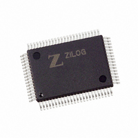
Z16F6411FI20SG Zilog, Z16F6411FI20SG Datasheet - Page 286

Z16F6411FI20SG
Manufacturer Part Number
Z16F6411FI20SG
Description
IC ZNEO MCU FLASH 64K 80QFP
Manufacturer
Zilog
Series
Encore!® ZNEOr
Datasheet
1.Z16F2800100ZCOG.pdf
(388 pages)
Specifications of Z16F6411FI20SG
Core Processor
ZNEO
Core Size
16-Bit
Speed
20MHz
Connectivity
EBI/EMI, I²C, IrDA, LIN, SPI, UART/USART
Peripherals
Brown-out Detect/Reset, DMA, POR, PWM, WDT
Number Of I /o
60
Program Memory Size
64KB (64K x 8)
Program Memory Type
FLASH
Ram Size
4K x 8
Voltage - Supply (vcc/vdd)
2.7 V ~ 3.6 V
Data Converters
A/D 12x10b
Oscillator Type
Internal
Operating Temperature
0°C ~ 70°C
Package / Case
80-BQFP
Processor Series
Z16F6x
Core
Zneo
Data Bus Width
16 bit
Data Ram Size
4 B
Interface Type
ESPI, I2C, UART
Maximum Clock Frequency
20 MHz
Number Of Programmable I/os
60
Number Of Timers
4
Operating Supply Voltage
2.7 V to 3.6 V
Maximum Operating Temperature
+ 70 C
Mounting Style
SMD/SMT
Development Tools By Supplier
Z16F2800100ZCOG
Minimum Operating Temperature
0 C
On-chip Adc
10 bit, 12 Channel
For Use With
770-1003 - ISP 4PORT FOR ZILOG ZNEO MCU269-4537 - DEV KIT FOR Z16F ZNEO
Lead Free Status / RoHS Status
Lead free / RoHS Compliant
Eeprom Size
-
Lead Free Status / Rohs Status
Details
Other names
269-4571
Available stocks
Company
Part Number
Manufacturer
Quantity
Price
Company:
Part Number:
Z16F6411FI20SG
Manufacturer:
LT
Quantity:
121
- Current page: 286 of 388
- Download datasheet (22Mb)
®
ZNEO
Z16F Series
Product Specification
270
Frames
A frame is a single buffer or a collection of buffers. Frame boundaries spans multiple
buffers.
Source Address Register
The source address register (SAR) points to the data to be transferred. Each time a transfer
occurs the SAR is selected to stay fixed or increment/decrement by the size of the transfer
(example 1, 2, 4). If we were sending data to a serial channel, the SAR points to the data to
be transferred and the SAR would be set to increment or decrement depending on the
order of data in the buffer (ascending or desending).
Destination Address Register
The destination address register (DAR) points to the location to store the data transferred
from the address pointed to by the SAR. Each time a transfer occurs the DAR is selected
to stay fixed or increment/decrement by the size of the transfer (for example, 1, 2, and 4).
When sending data to a serial channel, the DAR points to the data register of the serial
channel and is set to a fixed address. Each transfer is then sent to the serial channel data
register since the DAR would not change.
Transfer Length
The transfer length register (TXLN) is used to specify how many transfers need to occur to
transfer this buffer. If we were sending bytes to a serial channel, the value of the number of
bytes in the buffer pointed to by the SAR would be placed in this register. Each time a
transfer takes place this register is decremented by one. When the transfer length
decrements to zero, the buffer is complete and the DMA either stops or loads new control
information and addresses (see linked list description).
List Address Register
The list address register (LAR) is only used for linked list mode. The LAR points to a list
of descriptors (described below). This descriptor list contains setup information for each
buffer the DMA is to transfer. Linked list DMAs reduce the amount of overhead on the
CPU to service the DMA.
Descriptor
A Descriptor is a 16 byte field in the memory space. It needs to be aligned on 16 byte
boundaries (that is lower 4-bits of address is 0).
Table 141
provides the descriptor format.
PS022008-0810
P R E L I M I N A R Y
DMA Controller
Related parts for Z16F6411FI20SG
Image
Part Number
Description
Manufacturer
Datasheet
Request
R

Part Number:
Description:
Communication Controllers, ZILOG INTELLIGENT PERIPHERAL CONTROLLER (ZIP)
Manufacturer:
Zilog, Inc.
Datasheet:

Part Number:
Description:
KIT DEV FOR Z8 ENCORE 16K TO 64K
Manufacturer:
Zilog
Datasheet:

Part Number:
Description:
KIT DEV Z8 ENCORE XP 28-PIN
Manufacturer:
Zilog
Datasheet:

Part Number:
Description:
DEV KIT FOR Z8 ENCORE 8K/4K
Manufacturer:
Zilog
Datasheet:

Part Number:
Description:
KIT DEV Z8 ENCORE XP 28-PIN
Manufacturer:
Zilog
Datasheet:

Part Number:
Description:
DEV KIT FOR Z8 ENCORE 4K TO 8K
Manufacturer:
Zilog
Datasheet:

Part Number:
Description:
CMOS Z8 microcontroller. ROM 16 Kbytes, RAM 256 bytes, speed 16 MHz, 32 lines I/O, 3.0V to 5.5V
Manufacturer:
Zilog, Inc.
Datasheet:

Part Number:
Description:
Low-cost microcontroller. 512 bytes ROM, 61 bytes RAM, 8 MHz
Manufacturer:
Zilog, Inc.
Datasheet:

Part Number:
Description:
Z8 4K OTP Microcontroller
Manufacturer:
Zilog, Inc.
Datasheet:

Part Number:
Description:
CMOS SUPER8 ROMLESS MCU
Manufacturer:
Zilog, Inc.
Datasheet:

Part Number:
Description:
SL1866 CMOSZ8 OTP Microcontroller
Manufacturer:
Zilog, Inc.
Datasheet:

Part Number:
Description:
SL1866 CMOSZ8 OTP Microcontroller
Manufacturer:
Zilog, Inc.
Datasheet:

Part Number:
Description:
OTP (KB) = 1, RAM = 125, Speed = 12, I/O = 14, 8-bit Timers = 2, Comm Interfaces Other Features = Por, LV Protect, Voltage = 4.5-5.5V
Manufacturer:
Zilog, Inc.
Datasheet:

Part Number:
Description:
Manufacturer:
Zilog, Inc.
Datasheet:


