DEMO9S08LC60 Freescale Semiconductor, DEMO9S08LC60 Datasheet - Page 54
DEMO9S08LC60
Manufacturer Part Number
DEMO9S08LC60
Description
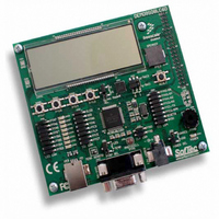
BOARD DEMO FOR 9S08LC60
Manufacturer
Freescale Semiconductor
Type
MCUr
Datasheets
1.DEMO9S08LC60.pdf
(360 pages)
2.DEMO9S08LC60.pdf
(32 pages)
3.DEMO9S08LC60.pdf
(2 pages)
Specifications of DEMO9S08LC60
Contents
Evaluation Board
Processor To Be Evaluated
MC9S08LC60
Interface Type
RS-232, USB
Silicon Manufacturer
Freescale
Core Architecture
HCS08
Core Sub-architecture
HCS08
Silicon Core Number
MC9S08
Silicon Family Name
S08LC
Rohs Compliant
Yes
For Use With/related Products
MC9S08LC60
Lead Free Status / RoHS Status
Lead free / RoHS Compliant


Chapter 4 Memory
NVPROT) must be programmed to logic 0 to enable block protection. Therefore the value 0xDE must be
programmed into NVPROT to protect addresses 0xE000 through 0xFFFF.
One use for block protection is to block protect an area of FLASH memory for a bootloader program. This
bootloader program can call a routine outside of FLASH that can be used to sector erase and re-program
the rest of the FLASH memory. The bootloader is protected even if MCU power is lost during an erase and
reprogram operation.
4.4.7
Whenever any block protection is enabled, the reset and interrupt vectors will be protected. Vector
redirection allows users to modify interrupt vector information without unprotecting bootloader and reset
vector space. Vector redirection is enabled by programming the FNORED bit in the NVOPT register
located at address 0xFFBF to zero. For redirection to occur, at least some portion but not all of the FLASH
memory must be block protected by programming the NVPROT register located at address 0xFFBD. All
of the interrupt vectors (memory locations 0xFFC0–0xFFFD) are redirected, while the reset vector
(0xFFFE–0xFFFF) is not. When more than 32K is protected, vector redirection must not be enabled.
For example, if 512 bytes of FLASH are protected, the protected address region is from 0xFE00 through
0xFFFF. The interrupt vectors (0xFFC0–0xFFFD) are redirected to the locations 0xFDC0–0xFDFD. Now,
if an SPI interrupt is taken for instance, the values in the locations 0xFDE0–0xFDE1 are used for the vector
instead of the values in the locations 0xFFE0–0xFFE1. This allows the user to reprogram the unprotected
portion of the FLASH with new program code including new interrupt vector values while leaving the
protected area, which includes the default vector locations, unchanged.
4.5
The MC9S08LC60 Series includes circuitry to prevent unauthorized access to the contents of FLASH and
RAM memory. When security is engaged, FLASH and RAM are considered secure resources. Direct-page
registers, high-page registers, and the background debug controller are considered unsecured resources.
Programs executing within secure memory have normal access to any MCU memory locations and
resources. Attempts to access a secure memory location with a program executing from an unsecured
memory space or through the background debug interface are blocked (writes are ignored and reads return
all 0s).
Security is engaged or disengaged based on the state of two nonvolatile register bits (SEC01:SEC00) in
the FOPT register. During reset, the contents of the nonvolatile location NVOPT are copied from FLASH
into the working FOPT register in high-page register space. A user engages security by programming the
NVOPT location which can be done at the same time the FLASH memory is programmed. The 1:0 state
disengages security while the other three combinations engage security. Notice the erased state (1:1)
54
Security
Vector Redirection
FPS7 FPS6 FPS5 FPS4 FPS3 FPS2 FPS1
A15
A14
A13
MC9S08LC60 Series Data Sheet: Technical Data, Rev. 4
Figure 4-4. Block Protection Mechanism
A12
A11
A10
A9
A8
1
A7 A6 A5 A4 A3 A2 A1 A0
1
1
1
1
1
1
Freescale Semiconductor
1
1
Related parts for DEMO9S08LC60
Image
Part Number
Description
Manufacturer
Datasheet
Request
R

Part Number:
Description:
Manufacturer:
Freescale Semiconductor, Inc
Datasheet:
Part Number:
Description:
Manufacturer:
Freescale Semiconductor, Inc
Datasheet:
Part Number:
Description:
Manufacturer:
Freescale Semiconductor, Inc
Datasheet:
Part Number:
Description:
Manufacturer:
Freescale Semiconductor, Inc
Datasheet:
Part Number:
Description:
Manufacturer:
Freescale Semiconductor, Inc
Datasheet:
Part Number:
Description:
Manufacturer:
Freescale Semiconductor, Inc
Datasheet:
Part Number:
Description:
Manufacturer:
Freescale Semiconductor, Inc
Datasheet:
Part Number:
Description:
Manufacturer:
Freescale Semiconductor, Inc
Datasheet:
Part Number:
Description:
Manufacturer:
Freescale Semiconductor, Inc
Datasheet:
Part Number:
Description:
Manufacturer:
Freescale Semiconductor, Inc
Datasheet:
Part Number:
Description:
Manufacturer:
Freescale Semiconductor, Inc
Datasheet:
Part Number:
Description:
Manufacturer:
Freescale Semiconductor, Inc
Datasheet:
Part Number:
Description:
Manufacturer:
Freescale Semiconductor, Inc
Datasheet:
Part Number:
Description:
Manufacturer:
Freescale Semiconductor, Inc
Datasheet:
Part Number:
Description:
Manufacturer:
Freescale Semiconductor, Inc
Datasheet: