DEMO9S08LC60 Freescale Semiconductor, DEMO9S08LC60 Datasheet - Page 226
DEMO9S08LC60
Manufacturer Part Number
DEMO9S08LC60
Description
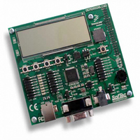
BOARD DEMO FOR 9S08LC60
Manufacturer
Freescale Semiconductor
Type
MCUr
Datasheets
1.DEMO9S08LC60.pdf
(360 pages)
2.DEMO9S08LC60.pdf
(32 pages)
3.DEMO9S08LC60.pdf
(2 pages)
Specifications of DEMO9S08LC60
Contents
Evaluation Board
Processor To Be Evaluated
MC9S08LC60
Interface Type
RS-232, USB
Silicon Manufacturer
Freescale
Core Architecture
HCS08
Core Sub-architecture
HCS08
Silicon Core Number
MC9S08
Silicon Family Name
S08LC
Rohs Compliant
Yes
For Use With/related Products
MC9S08LC60
Lead Free Status / RoHS Status
Lead free / RoHS Compliant


Chapter 12 Serial Communications Interface (S08SCIV3)
12.3
The SCI allows full-duplex, asynchronous, NRZ serial communication among the MCU and remote
devices, including other MCUs. The SCI comprises a baud rate generator, transmitter, and receiver block.
The transmitter and receiver operate independently, although they use the same baud rate generator. During
normal operation, the MCU monitors the status of the SCI, writes the data to be transmitted, and processes
received data. The following describes each of the blocks of the SCI.
12.3.1
As shown in
SCI communications require the transmitter and receiver (which typically derive baud rates from
independent clock sources) to use the same baud rate. Allowed tolerance on this baud frequency depends
on the details of how the receiver synchronizes to the leading edge of the start bit and how bit sampling is
performed.
The MCU resynchronizes to bit boundaries on every high-to-low transition, but in the worst case, there are
no such transitions in the full 10- or 11-bit time character frame so any mismatch in baud rate is
accumulated for the whole character time. For a Freescale Semiconductor SCI system whose bus
frequency is driven by a crystal, the allowed baud rate mismatch is about ±4.5 percent for 8-bit data format
and about ±4 percent for 9-bit data format. Although baud rate modulo divider settings do not always
produce baud rates that exactly match standard rates, it is normally possible to get within a few percent,
which is acceptable for reliable communications.
12.3.2
This section describes the overall block diagram for the SCI transmitter, as well as specialized functions
for sending break and idle characters. The transmitter block diagram is shown in
The transmitter output (TxD) idle state defaults to logic high (TXINV = 0 following reset). The transmitter
output is inverted by setting TXINV = 1. The transmitter is enabled by setting the TE bit in SCIC2. This
queues a preamble character that is one full character frame of the idle state. The transmitter then remains
idle until data is available in the transmit data buffer. Programs store data into the transmit data buffer by
writing to the SCI data register (SCID).
The central element of the SCI transmitter is the transmit shift register that is either 10 or 11 bits long
depending on the setting in the M control bit. For the remainder of this section, we will assume M = 0,
226
Functional Description
Baud Rate Generation
Transmitter Functional Description
Figure
BUSCLK
12-13, the clock source for the SCI baud rate generator is the bus-rate clock.
BAUD RATE GENERATOR
OFF IF [SBR12:SBR0] = 0
MC9S08LC60 Series Data Sheet: Technical Data, Rev. 4
MODULO DIVIDE BY
(1 THROUGH 8191)
Figure 12-13. SCI Baud Rate Generation
SBR12:SBR0
BAUD RATE =
DIVIDE BY
16
Rx SAMPLING CLOCK
(16 × BAUD RATE)
[SBR12:SBR0] × 16
BUSCLK
Tx BAUD RATE
Figure
Freescale Semiconductor
12-3.
Related parts for DEMO9S08LC60
Image
Part Number
Description
Manufacturer
Datasheet
Request
R

Part Number:
Description:
Manufacturer:
Freescale Semiconductor, Inc
Datasheet:
Part Number:
Description:
Manufacturer:
Freescale Semiconductor, Inc
Datasheet:
Part Number:
Description:
Manufacturer:
Freescale Semiconductor, Inc
Datasheet:
Part Number:
Description:
Manufacturer:
Freescale Semiconductor, Inc
Datasheet:
Part Number:
Description:
Manufacturer:
Freescale Semiconductor, Inc
Datasheet:
Part Number:
Description:
Manufacturer:
Freescale Semiconductor, Inc
Datasheet:
Part Number:
Description:
Manufacturer:
Freescale Semiconductor, Inc
Datasheet:
Part Number:
Description:
Manufacturer:
Freescale Semiconductor, Inc
Datasheet:
Part Number:
Description:
Manufacturer:
Freescale Semiconductor, Inc
Datasheet:
Part Number:
Description:
Manufacturer:
Freescale Semiconductor, Inc
Datasheet:
Part Number:
Description:
Manufacturer:
Freescale Semiconductor, Inc
Datasheet:
Part Number:
Description:
Manufacturer:
Freescale Semiconductor, Inc
Datasheet:
Part Number:
Description:
Manufacturer:
Freescale Semiconductor, Inc
Datasheet:
Part Number:
Description:
Manufacturer:
Freescale Semiconductor, Inc
Datasheet:
Part Number:
Description:
Manufacturer:
Freescale Semiconductor, Inc
Datasheet: