DEMO9S08LC60 Freescale Semiconductor, DEMO9S08LC60 Datasheet - Page 53
DEMO9S08LC60
Manufacturer Part Number
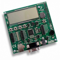
DEMO9S08LC60
Description
BOARD DEMO FOR 9S08LC60
Manufacturer
Freescale Semiconductor
Type
MCUr
Datasheets
1.DEMO9S08LC60.pdf
(360 pages)
2.DEMO9S08LC60.pdf
(32 pages)
3.DEMO9S08LC60.pdf
(2 pages)
Specifications of DEMO9S08LC60
Contents
Evaluation Board
Processor To Be Evaluated
MC9S08LC60
Interface Type
RS-232, USB
Silicon Manufacturer
Freescale
Core Architecture
HCS08
Core Sub-architecture
HCS08
Silicon Core Number
MC9S08
Silicon Family Name
S08LC
Rohs Compliant
Yes
For Use With/related Products
MC9S08LC60
Lead Free Status / RoHS Status
Lead free / RoHS Compliant


4.4.5
An access error occurs whenever the command execution protocol is violated. Any of the following
specific actions will cause the access error flag (FACCERR) in FSTAT to be set. FACCERR must be
cleared by writing a 1 to FACCERR in FSTAT before any command can be processed.
4.4.6
The block protection feature prevents the protected region of FLASH from program or erase changes.
Block protection is controlled through the FLASH Protection Register (FPROT). When enabled, block
protection begins at any 512 byte boundary below the last address of FLASH, 0xFFFF. (see
“FLASH Protection Register (FPROT and
After exit from reset, FPROT is loaded with the contents of the NVPROT location which is in the
nonvolatile register block of the FLASH memory. In user mode, if FPDIS is set, all FPROT bits are
writeable. In user mode, if FPDIS is clear, the FPS bits are writeable as long as the size of the protected
region is being increased. Because NVPROT is within the last sector of FLASH, if any amount of memory
is protected, NVPROT is itself protected and cannot be altered (intentionally or unintentionally) by the
application software. FPROT can be written through background debug commands, which provide a way
to erase and reprogram protected FLASH memory.
The block protection mechanism is illustrated in
last address of unprotected memory. This address is formed by concatenating FPS7:FPS1 with logic 1 bits
as shown. For example, in order to protect the last 8192 bytes of memory (addresses 0xE000 through
0xFFFF), the FPS bits must be set to 1101 111 which results in the value 0xDFFF as the last address of
unprotected memory. In addition to programming the FPS bits to the appropriate value, FPDIS (bit 0 of
Freescale Semiconductor
•
•
•
•
•
•
•
•
•
•
Writing to a FLASH address before the internal FLASH clock frequency has been set by writing
to the FCDIV register
command buffer is empty.)
Writing a second time to a FLASH address before launching the previous command (There is only
one write to FLASH for every command.)
Writing a second time to FCMD before launching the previous command (There is only one write
to FCMD for every command.)
Writing to any FLASH control register other than FCMD after writing to a FLASH address
Writing any command code other than the five allowed codes (0x05, 0x20, 0x25, 0x40, or 0x41)
to FCMD
Accessing (read or write) any FLASH control register other than the write to FSTAT (to clear
FCBEF and launch the command) after writing the command to FCMD
The MCU enters stop mode while a program or erase command is in progress (The command is
aborted.)
Writing the byte program, burst program, or page erase command code (0x20, 0x25, or 0x40) with
a background debug command while the MCU is secured (The background debug controller can
do blank check and mass erase commands only while the MCU is secure.)
Writing 0 to FCBEF to cancel a partial command
Writing to a FLASH address while FCBEF is not set (A new command cannot be started until the
Access Errors
FLASH Block Protection
MC9S08LC60 Series Data Sheet: Technical Data, Rev. 4
NVPROT)”).
Figure
4-4. The FPS bits are used as the upper bits of the
Chapter 4 Memory
Section 4.6.4,
53
Related parts for DEMO9S08LC60
Image
Part Number
Description
Manufacturer
Datasheet
Request
R

Part Number:
Description:
Manufacturer:
Freescale Semiconductor, Inc
Datasheet:
Part Number:
Description:
Manufacturer:
Freescale Semiconductor, Inc
Datasheet:
Part Number:
Description:
Manufacturer:
Freescale Semiconductor, Inc
Datasheet:
Part Number:
Description:
Manufacturer:
Freescale Semiconductor, Inc
Datasheet:
Part Number:
Description:
Manufacturer:
Freescale Semiconductor, Inc
Datasheet:
Part Number:
Description:
Manufacturer:
Freescale Semiconductor, Inc
Datasheet:
Part Number:
Description:
Manufacturer:
Freescale Semiconductor, Inc
Datasheet:
Part Number:
Description:
Manufacturer:
Freescale Semiconductor, Inc
Datasheet:
Part Number:
Description:
Manufacturer:
Freescale Semiconductor, Inc
Datasheet:
Part Number:
Description:
Manufacturer:
Freescale Semiconductor, Inc
Datasheet:
Part Number:
Description:
Manufacturer:
Freescale Semiconductor, Inc
Datasheet:
Part Number:
Description:
Manufacturer:
Freescale Semiconductor, Inc
Datasheet:
Part Number:
Description:
Manufacturer:
Freescale Semiconductor, Inc
Datasheet:
Part Number:
Description:
Manufacturer:
Freescale Semiconductor, Inc
Datasheet:
Part Number:
Description:
Manufacturer:
Freescale Semiconductor, Inc
Datasheet: