DEMO9S08LC60 Freescale Semiconductor, DEMO9S08LC60 Datasheet - Page 150
DEMO9S08LC60
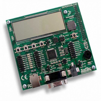
Manufacturer Part Number
DEMO9S08LC60
Description
BOARD DEMO FOR 9S08LC60
Manufacturer
Freescale Semiconductor
Type
MCUr
Datasheets
1.DEMO9S08LC60.pdf
(360 pages)
2.DEMO9S08LC60.pdf
(32 pages)
3.DEMO9S08LC60.pdf
(2 pages)
Specifications of DEMO9S08LC60
Contents
Evaluation Board
Processor To Be Evaluated
MC9S08LC60
Interface Type
RS-232, USB
Silicon Manufacturer
Freescale
Core Architecture
HCS08
Core Sub-architecture
HCS08
Silicon Core Number
MC9S08
Silicon Family Name
S08LC
Rohs Compliant
Yes
For Use With/related Products
MC9S08LC60
Lead Free Status / RoHS Status
Lead free / RoHS Compliant


Chapter 9 Liquid Crystal Display Driver (S08LCDV1)
9.4.3.1
To configure all LCD segments to blink regardless of the contents of the LCDRAM bits while
LCDDRMS = 1, the BLKMODE bit in the LCDBCTL control register must to set to 1. To configure
individual LCD segments to blink, the BLKMODE bit in the LCDBCTL control register must be
deasserted.
If BLKMODE = 0, asserting the LCDRAM FP[n]BP[x] bits while LCDDRMS = 0 and LCDDRMS = 1
enables the LCD segment connected between FP[n] and BP[x] to blink when BLINK = 1. Each LCDRAM
register controls two frontplane drivers.
9.4.3.2
The LCD module waveform base clock is the basis for the calculation of the LCD module blink frequency.
The LCD module blink frequency is equal to the LCD module waveform base clock divided by the
BRATE[2:0] divider.
BRATE[2:0] and LCLK[2:0].
1 Shaded table entries are out of specification and are not valid
9.4.4
This section describes the LCD charge pump, voltage divider, and LCD power supply configuration
options.
The VSUPPLY[1:0] bit field in the LCDSUPPLY register is used to configure the LCD module power
supply source. VSUPPLY[1:0] indicates the state of internal signals used to configure power switches as
shown in the Table in
operational modes for the LCD module including configuration of the LCD module power supply source
using internal V
150
LCLK[2:0]
Figure 9-17
0
1
2
3
4
5
6
7
LCD Charge Pump, Voltage Divider, and Power Supply Operation
LCD Segment Blinking
Blink Frequency
DD
Frequency (Hz)
LCD Base
or an external supply.
provides a block diagram for the LCD charge pump and a V
2049.3
1024.7
Table 9-17
512.3
256.2
128.1
64.0
32.0
16.0
Figure
MC9S08LC60 Series Data Sheet: Technical Data, Rev. 4
9-17. The block diagram in
Table 9-17. Blink Frequency Calculations
shows LCD module blink frequency calculations for all values of
(
Blink Rate = LCD Base (Hz) ÷ Blink Divider)
64.0
32.0
16.0
8.00
4.00
2.00
1.00
0.50
32
32.0
16.0
8.00
4.00
2.00
1.00
0.50
0.25
64
16.0
8.00
4.00
2.00
1.00
0.50
0.25
0.13
128
Blink Divider = 2
Figure 9-17
Blink Frequency
8.00
4.00
2.00
1.00
0.50
0.25
0.13
0.06
256
(5+ BRATE[2:0])
4.00
2.00
1.00
0.50
0.25
0.13
0.06
0.03
512
illustrates several potential
1024
2.00
1.00
0.50
0.25
0.13
0.06
0.03
0.02
LCD
Freescale Semiconductor
voltage divider.
2048
1.00
0.50
0.25
0.13
0.06
0.03
0.02
0.01
4096
0.50
0.25
0.13
0.06
0.03
0.02
0.01
0.00
Related parts for DEMO9S08LC60
Image
Part Number
Description
Manufacturer
Datasheet
Request
R

Part Number:
Description:
Manufacturer:
Freescale Semiconductor, Inc
Datasheet:
Part Number:
Description:
Manufacturer:
Freescale Semiconductor, Inc
Datasheet:
Part Number:
Description:
Manufacturer:
Freescale Semiconductor, Inc
Datasheet:
Part Number:
Description:
Manufacturer:
Freescale Semiconductor, Inc
Datasheet:
Part Number:
Description:
Manufacturer:
Freescale Semiconductor, Inc
Datasheet:
Part Number:
Description:
Manufacturer:
Freescale Semiconductor, Inc
Datasheet:
Part Number:
Description:
Manufacturer:
Freescale Semiconductor, Inc
Datasheet:
Part Number:
Description:
Manufacturer:
Freescale Semiconductor, Inc
Datasheet:
Part Number:
Description:
Manufacturer:
Freescale Semiconductor, Inc
Datasheet:
Part Number:
Description:
Manufacturer:
Freescale Semiconductor, Inc
Datasheet:
Part Number:
Description:
Manufacturer:
Freescale Semiconductor, Inc
Datasheet:
Part Number:
Description:
Manufacturer:
Freescale Semiconductor, Inc
Datasheet:
Part Number:
Description:
Manufacturer:
Freescale Semiconductor, Inc
Datasheet:
Part Number:
Description:
Manufacturer:
Freescale Semiconductor, Inc
Datasheet:
Part Number:
Description:
Manufacturer:
Freescale Semiconductor, Inc
Datasheet: