DEMO9S08LC60 Freescale Semiconductor, DEMO9S08LC60 Datasheet - Page 175
DEMO9S08LC60
Manufacturer Part Number
DEMO9S08LC60
Description
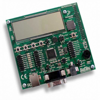
BOARD DEMO FOR 9S08LC60
Manufacturer
Freescale Semiconductor
Type
MCUr
Datasheets
1.DEMO9S08LC60.pdf
(360 pages)
2.DEMO9S08LC60.pdf
(32 pages)
3.DEMO9S08LC60.pdf
(2 pages)
Specifications of DEMO9S08LC60
Contents
Evaluation Board
Processor To Be Evaluated
MC9S08LC60
Interface Type
RS-232, USB
Silicon Manufacturer
Freescale
Core Architecture
HCS08
Core Sub-architecture
HCS08
Silicon Core Number
MC9S08
Silicon Family Name
S08LC
Rohs Compliant
Yes
For Use With/related Products
MC9S08LC60
Lead Free Status / RoHS Status
Lead free / RoHS Compliant


1
10.4
Refer to the direct-page register summary in the
assignments for all ICG registers. This section refers to registers and control bits only by their names. A
Freescale-provided equate or header file is used to translate these names into the appropriate absolute
addresses.
10.4.1
Freescale Semiconductor
This bit can be written only once after reset. Additional writes are ignored.
Reset
RANGE
REFS
CLKS
Field
HGO
4:3
7
6
5
W
R
Register Definition
ICG Control Register 1 (ICGC1)
HGO
High Gain Oscillator Select — The HGO bit is used to select between low power operation and high gain
operation for improved noise immunity. This bit is write-once after reset.
0 Oscillator configured for low power operation.
1 Oscillator configured for high gain operation.
Frequency Range Select — The RANGE bit controls the oscillator, reference divider, and FLL loop prescaler
multiplication factor (P). It selects one of two reference frequency ranges for the ICG. The RANGE bit is
write-once after a reset. The RANGE bit only has an effect in FLL engaged external and FLL bypassed external
modes.
0 Oscillator configured for low frequency range. FLL loop prescale factor P is 64.
1 Oscillator configured for high frequency range. FLL loop prescale factor P is 1.
External Reference Select — The REFS bit controls the external reference clock source for ICGERCLK. The
REFS bit is write-once after a reset.
0 External clock requested.
1 Oscillator using crystal or resonator requested.
Clock Mode Select — The CLKS bits control the clock mode as described below. If FLL bypassed external is
requested, it will not be selected until ERCS = 1. If the ICG enters off mode, the CLKS bits will remain
unchanged. Writes to the CLKS bits will not take effect if a previous write is not complete.
00 Self-clocked
01 FLL engaged, internal reference
10 FLL bypassed, external reference
11 FLL engaged, external reference
The CLKS bits are writable at any time, unless the first write after a reset was CLKS = 0X, the CLKS bits cannot
be written to 1X until after the next reset (because the EXTAL pin was not reserved).
0
7
1
= Unimplemented or Reserved
RANGE
1
6
MC9S08LC60 Series Data Sheet: Technical Data, Rev. 4
Table 10-1. ICGC1 Register Field Descriptions
Figure 10-6. ICG Control Register 1 (ICGC1)
REFS
0
5
Memory
0
4
Description
CLKS
chapter of this data sheet for the absolute address
3
0
Chapter 10 Internal Clock Generator (S08ICGV4)
OSCSTEN
1
2
LOCD
0
1
0
0
0
175
Related parts for DEMO9S08LC60
Image
Part Number
Description
Manufacturer
Datasheet
Request
R

Part Number:
Description:
Manufacturer:
Freescale Semiconductor, Inc
Datasheet:
Part Number:
Description:
Manufacturer:
Freescale Semiconductor, Inc
Datasheet:
Part Number:
Description:
Manufacturer:
Freescale Semiconductor, Inc
Datasheet:
Part Number:
Description:
Manufacturer:
Freescale Semiconductor, Inc
Datasheet:
Part Number:
Description:
Manufacturer:
Freescale Semiconductor, Inc
Datasheet:
Part Number:
Description:
Manufacturer:
Freescale Semiconductor, Inc
Datasheet:
Part Number:
Description:
Manufacturer:
Freescale Semiconductor, Inc
Datasheet:
Part Number:
Description:
Manufacturer:
Freescale Semiconductor, Inc
Datasheet:
Part Number:
Description:
Manufacturer:
Freescale Semiconductor, Inc
Datasheet:
Part Number:
Description:
Manufacturer:
Freescale Semiconductor, Inc
Datasheet:
Part Number:
Description:
Manufacturer:
Freescale Semiconductor, Inc
Datasheet:
Part Number:
Description:
Manufacturer:
Freescale Semiconductor, Inc
Datasheet:
Part Number:
Description:
Manufacturer:
Freescale Semiconductor, Inc
Datasheet:
Part Number:
Description:
Manufacturer:
Freescale Semiconductor, Inc
Datasheet:
Part Number:
Description:
Manufacturer:
Freescale Semiconductor, Inc
Datasheet: