DEMO9S08LC60 Freescale Semiconductor, DEMO9S08LC60 Datasheet - Page 315
DEMO9S08LC60
Manufacturer Part Number
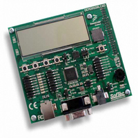
DEMO9S08LC60
Description
BOARD DEMO FOR 9S08LC60
Manufacturer
Freescale Semiconductor
Type
MCUr
Datasheets
1.DEMO9S08LC60.pdf
(360 pages)
2.DEMO9S08LC60.pdf
(32 pages)
3.DEMO9S08LC60.pdf
(2 pages)
Specifications of DEMO9S08LC60
Contents
Evaluation Board
Processor To Be Evaluated
MC9S08LC60
Interface Type
RS-232, USB
Silicon Manufacturer
Freescale
Core Architecture
HCS08
Core Sub-architecture
HCS08
Silicon Core Number
MC9S08
Silicon Family Name
S08LC
Rohs Compliant
Yes
For Use With/related Products
MC9S08LC60
Lead Free Status / RoHS Status
Lead free / RoHS Compliant


Active BDM:
17.4.1.1
This register can be read or written by serial BDC commands (READ_STATUS and WRITE_CONTROL)
but is not accessible to user programs because it is not located in the normal memory map of the MCU.
Reset in
Freescale Semiconductor
Normal
Reset
BDMACT
BKPTEN
ENBDM
CLKSW
Field
FTS
W
7
6
5
4
3
R
ENBDM
Enable BDM (Permit Active Background Mode) — Typically, this bit is written to 1 by the debug host shortly
after the beginning of a debug session or whenever the debug host resets the target and remains 1 until a normal
reset clears it.
0 BDM cannot be made active (non-intrusive commands still allowed)
1 BDM can be made active to allow active background mode commands
Background Mode Active Status — This is a read-only status bit.
0 BDM not active (user application program running)
1 BDM active and waiting for serial commands
BDC Breakpoint Enable — If this bit is clear, the BDC breakpoint is disabled and the FTS (force tag select)
control bit and BDCBKPT match register are ignored.
0 BDC breakpoint disabled
1 BDC breakpoint enabled
Force/Tag Select — When FTS = 1, a breakpoint is requested whenever the CPU address bus matches the
BDCBKPT match register. When FTS = 0, a match between the CPU address bus and the BDCBKPT register
causes the fetched opcode to be tagged. If this tagged opcode ever reaches the end of the instruction queue,
the CPU enters active background mode rather than executing the tagged opcode.
0 Tag opcode at breakpoint address and enter active background mode if CPU attempts to execute that
1 Breakpoint match forces active background mode at next instruction boundary (address need not be an
Select Source for BDC Communications Clock — CLKSW defaults to 0, which selects the alternate BDC
clock source.
0 Alternate BDC clock source
1 MCU bus clock
0
1
7
BDC Status and Control Register (BDCSCR)
instruction
opcode)
= Unimplemented or Reserved
BDMACT
Figure 17-5. BDC Status and Control Register (BDCSCR)
0
1
6
MC9S08LC60 Series Data Sheet: Technical Data, Rev. 4
Table 17-2. BDCSCR Register Field Descriptions
BKPTEN
0
0
5
FTS
0
0
4
Description
CLKSW
0
1
3
WS
0
0
2
Chapter 17 Development Support
WSF
1
0
0
DVF
0
0
0
315
Related parts for DEMO9S08LC60
Image
Part Number
Description
Manufacturer
Datasheet
Request
R

Part Number:
Description:
Manufacturer:
Freescale Semiconductor, Inc
Datasheet:
Part Number:
Description:
Manufacturer:
Freescale Semiconductor, Inc
Datasheet:
Part Number:
Description:
Manufacturer:
Freescale Semiconductor, Inc
Datasheet:
Part Number:
Description:
Manufacturer:
Freescale Semiconductor, Inc
Datasheet:
Part Number:
Description:
Manufacturer:
Freescale Semiconductor, Inc
Datasheet:
Part Number:
Description:
Manufacturer:
Freescale Semiconductor, Inc
Datasheet:
Part Number:
Description:
Manufacturer:
Freescale Semiconductor, Inc
Datasheet:
Part Number:
Description:
Manufacturer:
Freescale Semiconductor, Inc
Datasheet:
Part Number:
Description:
Manufacturer:
Freescale Semiconductor, Inc
Datasheet:
Part Number:
Description:
Manufacturer:
Freescale Semiconductor, Inc
Datasheet:
Part Number:
Description:
Manufacturer:
Freescale Semiconductor, Inc
Datasheet:
Part Number:
Description:
Manufacturer:
Freescale Semiconductor, Inc
Datasheet:
Part Number:
Description:
Manufacturer:
Freescale Semiconductor, Inc
Datasheet:
Part Number:
Description:
Manufacturer:
Freescale Semiconductor, Inc
Datasheet:
Part Number:
Description:
Manufacturer:
Freescale Semiconductor, Inc
Datasheet: