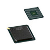
PNX1500E NXP Semiconductors, PNX1500E Datasheet - Page 76

PNX1500E
Manufacturer Part Number
PNX1500E
Description
Manufacturer
NXP Semiconductors
Datasheet
1.PNX1500E.pdf
(828 pages)
Specifications of PNX1500E
Lead Free Status / Rohs Status
Not Compliant
Available stocks
Company
Part Number
Manufacturer
Quantity
Price
Company:
Part Number:
PNX1500E
Manufacturer:
NORTEL
Quantity:
1 000
- Current page: 76 of 828
- Download datasheet (4Mb)
NXP Semiconductors
Volume 1 of 1
PNX15XX_PNX952X_SER_N_4
Product data sheet
10.3 DDR SDRAM interface
All the key components (the analog bypass capacitor and crystal capacitors) are on
the PCB connected to the free-floating analog VSSA_1.2 net
Designing a proper DDR SDRAM interface with the PNX1500 system that
guarantees correct signal integrity and timing margins (even at 200 MHz, i.e.
DDR400) can be achieved by implementing the following board level design rules:
Figure 27: Digital VDD Power Supply to Analog VDDA/VSSA_1.2 Power Supply Filter
Figure 28: Digital VDD Power Supply to Analog VDDA/VSSA_1.2 Power Supply Filter
•
•
•
50
must be adjusted to meet the 50
drivers must be fine tuned to limit undershoot and/or overshoot over traces with
50
‘T’ shape connection when a signal must be connected to two (or more) memory
devices. The bar of the ‘T’ should have impedance higher than 50
compensate for the trace split. 70
the ‘T’ is less than half of the ‘leg’ of the ‘T’.
Each DQS/DQM/DATA byte lane should remain on the same plane and go
through the same amount of VIAs.
trace impedance. The width of the PCB trace as well as the dielectric layer
impedance. This should guarantee high quality signal integrity.
V
V
DD
DD
Rev. 4.0 — 03 December 2007
100
100
27 MHz
V
DD
47 F
47 F
impedance traces. The PNX1500 SSTL_2
is recommended but not required if the bar of
0.1 F
0.1 F
N.C.
27 MHz
PNX15xx/952x Series
Chapter 1: Integrated Circuit Data
VDDA
XTAL_IN
XTAL_OUT
VSSA_1.2
VDDA
VSSA_1.2
XTAL_IN
XTAL_OUT
PNX1500
PNX1500
(Figure
© NXP B.V. 2007. All rights reserved.
27,
in order to
Figure
28).
1-76
Related parts for PNX1500E
Image
Part Number
Description
Manufacturer
Datasheet
Request
R
Part Number:
Description:
NXP Semiconductors designed the LPC2420/2460 microcontroller around a 16-bit/32-bitARM7TDMI-S CPU core with real-time debug interfaces that include both JTAG andembedded trace
Manufacturer:
NXP Semiconductors
Datasheet:

Part Number:
Description:
NXP Semiconductors designed the LPC2458 microcontroller around a 16-bit/32-bitARM7TDMI-S CPU core with real-time debug interfaces that include both JTAG andembedded trace
Manufacturer:
NXP Semiconductors
Datasheet:
Part Number:
Description:
NXP Semiconductors designed the LPC2468 microcontroller around a 16-bit/32-bitARM7TDMI-S CPU core with real-time debug interfaces that include both JTAG andembedded trace
Manufacturer:
NXP Semiconductors
Datasheet:
Part Number:
Description:
NXP Semiconductors designed the LPC2470 microcontroller, powered by theARM7TDMI-S core, to be a highly integrated microcontroller for a wide range ofapplications that require advanced communications and high quality graphic displays
Manufacturer:
NXP Semiconductors
Datasheet:
Part Number:
Description:
NXP Semiconductors designed the LPC2478 microcontroller, powered by theARM7TDMI-S core, to be a highly integrated microcontroller for a wide range ofapplications that require advanced communications and high quality graphic displays
Manufacturer:
NXP Semiconductors
Datasheet:
Part Number:
Description:
The Philips Semiconductors XA (eXtended Architecture) family of 16-bit single-chip microcontrollers is powerful enough to easily handle the requirements of high performance embedded applications, yet inexpensive enough to compete in the market for hi
Manufacturer:
NXP Semiconductors
Datasheet:
Part Number:
Description:
The XA-S3 device is a member of Philips Semiconductors? XA(eXtended Architecture) family of high performance 16-bitsingle-chip microcontrollers
Manufacturer:
NXP Semiconductors
Datasheet:

Part Number:
Description:
The NXP BlueStreak LH75401/LH75411 family consists of two low-cost 16/32-bit System-on-Chip (SoC) devices
Manufacturer:
NXP Semiconductors
Datasheet:

Part Number:
Description:
The NXP LPC3130/3131 combine an 180 MHz ARM926EJ-S CPU core, high-speed USB2
Manufacturer:
NXP Semiconductors
Datasheet:

Part Number:
Description:
The NXP LPC3141 combine a 270 MHz ARM926EJ-S CPU core, High-speed USB 2
Manufacturer:
NXP Semiconductors

Part Number:
Description:
The NXP LPC3143 combine a 270 MHz ARM926EJ-S CPU core, High-speed USB 2
Manufacturer:
NXP Semiconductors

Part Number:
Description:
The NXP LPC3152 combines an 180 MHz ARM926EJ-S CPU core, High-speed USB 2
Manufacturer:
NXP Semiconductors

Part Number:
Description:
The NXP LPC3154 combines an 180 MHz ARM926EJ-S CPU core, High-speed USB 2
Manufacturer:
NXP Semiconductors

Part Number:
Description:
Standard level N-channel enhancement mode Field-Effect Transistor (FET) in a plastic package using NXP High-Performance Automotive (HPA) TrenchMOS technology
Manufacturer:
NXP Semiconductors
Datasheet:


