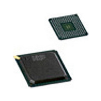
PNX1500E NXP Semiconductors, PNX1500E Datasheet - Page 28

PNX1500E
Manufacturer Part Number
PNX1500E
Description
Manufacturer
NXP Semiconductors
Datasheet
1.PNX1500E.pdf
(828 pages)
Specifications of PNX1500E
Lead Free Status / Rohs Status
Not Compliant
Available stocks
Company
Part Number
Manufacturer
Quantity
Price
Company:
Part Number:
PNX1500E
Manufacturer:
NORTEL
Quantity:
1 000
- Current page: 28 of 828
- Download datasheet (4Mb)
NXP Semiconductors
Volume 1 of 1
Table 4: PNX1500 Interface
PNX15XX_PNX952X_SER_N_4
Product data sheet
Pin Name
System Clock
XTAL_IN
XTAL_OUT
PCI_SYS_CLK
Miscellaneous System Interface
POR_IN_N
RESET_IN_N
SYS_RST_OUT_N
RESERVED
Main Memory Interface (DDR SDRAM controller)
Refer to
Section 10.3 on page 1-76
BGA
Ball
AB23 BPT3MCHDT5V
D11
D10
E25
A11
D9
C7
Remark: The pull-down in the BPT3MCHDT5V pads is NOT strong enough to
actually pull down a 5-V TTL input. Instead the TTL input pin sees a ‘1’.
Pad
Type
BPT3MCHT5V
BPT3MCHT5V
BPX2T14MCP
BPX2T14MCP
for board design guidelines
APIO1V2
APIO1V2
Rev. 4.0 — 03 December 2007
I/O
Type
OUT
OUT
OUT
I/O
IN
IN
IN
GPIO
#
-
-
-
-
-
-
-
P Description
U This clock is intended for use as the PCI clock in
U PNX1500 Power On Reset input. Asserting this
U PNX1500 reset input. Asserting this input low
U Active low peripheral reset output. This output is
D Reserved for future expansion. It has to be left
- PNX1500 main input clock. All internal clocks are
- Crystal oscillator output. Connect external crystal
derived from this 27 MHz input reference clock.
The crystal should be placed as close as possible
to the package. Refer to
board level connections.
This input follows the operating range of V
between this pin and XTAL_IN. Refer to
and
simple PNX1500 PCI configurations. It outputs a
33.23 MHz clock. A board level 27-33
resistor is recommended to reduce ringing.
input low triggers the hardware reset function of the
PNX1500 (including the JTAG state machine).
This pin can typically be connected to an on-board
reset upon voltage drop. It is active low. Upon
asserting this reset input, the PNX1500 asserts
SYS_RST_OUT_N to reset the attached peripheral
chips. This pin can also be tied to the PCI_RST
signal in a PCI bus systems. This pin is 5 V tolerant
input.
triggers the hardware reset function of the
PNX1500 (This does not reset the JTAG state
machine). Upon asserting this reset input,
PNX1500 asserts SYS_RST_OUT_N to reset
attached peripheral chips. This pin can also be tied
to the PCI_RST signal in a PCI bus systems.
With respect to the POR_IN_N reset pin, this pin
can be used has a warm reset. For most
applications, both reset pins can be tied together. it
is active low. This pin is 5 V tolerant input.
asserted upon any PNX1500 reset (hardware,
watchdog timer or software), and de-asserted by
PNX1500 system software. It is intended to be used
as a reset for external peripherals.
unconnected at the board level for normal
operation.
Figure 27
PNX15xx/952x Series
Chapter 1: Integrated Circuit Data
for board level connections.
Figure 1
© NXP B.V. 2007. All rights reserved.
and
Figure 27
Figure 1
series
DD
for
.
1-28
Related parts for PNX1500E
Image
Part Number
Description
Manufacturer
Datasheet
Request
R
Part Number:
Description:
NXP Semiconductors designed the LPC2420/2460 microcontroller around a 16-bit/32-bitARM7TDMI-S CPU core with real-time debug interfaces that include both JTAG andembedded trace
Manufacturer:
NXP Semiconductors
Datasheet:

Part Number:
Description:
NXP Semiconductors designed the LPC2458 microcontroller around a 16-bit/32-bitARM7TDMI-S CPU core with real-time debug interfaces that include both JTAG andembedded trace
Manufacturer:
NXP Semiconductors
Datasheet:
Part Number:
Description:
NXP Semiconductors designed the LPC2468 microcontroller around a 16-bit/32-bitARM7TDMI-S CPU core with real-time debug interfaces that include both JTAG andembedded trace
Manufacturer:
NXP Semiconductors
Datasheet:
Part Number:
Description:
NXP Semiconductors designed the LPC2470 microcontroller, powered by theARM7TDMI-S core, to be a highly integrated microcontroller for a wide range ofapplications that require advanced communications and high quality graphic displays
Manufacturer:
NXP Semiconductors
Datasheet:
Part Number:
Description:
NXP Semiconductors designed the LPC2478 microcontroller, powered by theARM7TDMI-S core, to be a highly integrated microcontroller for a wide range ofapplications that require advanced communications and high quality graphic displays
Manufacturer:
NXP Semiconductors
Datasheet:
Part Number:
Description:
The Philips Semiconductors XA (eXtended Architecture) family of 16-bit single-chip microcontrollers is powerful enough to easily handle the requirements of high performance embedded applications, yet inexpensive enough to compete in the market for hi
Manufacturer:
NXP Semiconductors
Datasheet:
Part Number:
Description:
The XA-S3 device is a member of Philips Semiconductors? XA(eXtended Architecture) family of high performance 16-bitsingle-chip microcontrollers
Manufacturer:
NXP Semiconductors
Datasheet:

Part Number:
Description:
The NXP BlueStreak LH75401/LH75411 family consists of two low-cost 16/32-bit System-on-Chip (SoC) devices
Manufacturer:
NXP Semiconductors
Datasheet:

Part Number:
Description:
The NXP LPC3130/3131 combine an 180 MHz ARM926EJ-S CPU core, high-speed USB2
Manufacturer:
NXP Semiconductors
Datasheet:

Part Number:
Description:
The NXP LPC3141 combine a 270 MHz ARM926EJ-S CPU core, High-speed USB 2
Manufacturer:
NXP Semiconductors

Part Number:
Description:
The NXP LPC3143 combine a 270 MHz ARM926EJ-S CPU core, High-speed USB 2
Manufacturer:
NXP Semiconductors

Part Number:
Description:
The NXP LPC3152 combines an 180 MHz ARM926EJ-S CPU core, High-speed USB 2
Manufacturer:
NXP Semiconductors

Part Number:
Description:
The NXP LPC3154 combines an 180 MHz ARM926EJ-S CPU core, High-speed USB 2
Manufacturer:
NXP Semiconductors

Part Number:
Description:
Standard level N-channel enhancement mode Field-Effect Transistor (FET) in a plastic package using NXP High-Performance Automotive (HPA) TrenchMOS technology
Manufacturer:
NXP Semiconductors
Datasheet:


