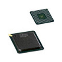
PNX1500E NXP Semiconductors, PNX1500E Datasheet - Page 501

PNX1500E
Manufacturer Part Number
PNX1500E
Description
Manufacturer
NXP Semiconductors
Datasheet
1.PNX1500E.pdf
(828 pages)
Specifications of PNX1500E
Lead Free Status / Rohs Status
Not Compliant
Available stocks
Company
Part Number
Manufacturer
Quantity
Price
Company:
Part Number:
PNX1500E
Manufacturer:
NORTEL
Quantity:
1 000
- Current page: 501 of 828
- Download datasheet (4Mb)
NXP Semiconductors
Volume 1 of 1
4. Register Descriptions
Table 2: Register Summary
Table 3: Fast general purpose INput (FGPI)
PNX15XX_PNX952X_SER_N_4
Product data sheet
Offset
0x07,0000
0x07,0004
0x07,0008
0x07,000C
0x07,0010
0x07,0014
0x07,0018
0x07,001C
0x07,0020
0x07,0024
0x07,0028 -
0x07,0FDC
0x07,0FE0
0x07,0FE4
0x07,0FE8
0x07,0FEC
0x07,0FF0
0x07,0FF4
0x07,0FF8
0x07,0FFC
Bit
FPGI Registers
Offset 0x07,0000
31:15
14
13
Symbol
Reserved
POLARITY_CLK
CAPTURE_ENABLE_2
Name
FGPI_CTL
FGPI_BASE1
FGPI_BASE2
FGPI_SIZE
FGPI_REC_SIZE
FGPI_STRIDE
FGPI_NREC1
FGPI_NREC2
FGPI_THRESH1
FGPI_THRESH2
reserved
FGPI_IR_STATUS
FGPI_IR_ENA
FGPI_IR_CLR
FGPI_IR_SET
FGPI_SOFT_RST
FGPI_IF_DIS
FGPI_MOD_ID_EXT
FGPI_MOD_ID
4.1 Mode Registers
FGPI_CTL
Acces
s
R
R/W
R/W
Clock
Domain
fgpi
mmio
mmio
fgpi
fgpi
fgpi
mmio
mmio
fgpi
fgpi
n/a
mmio
mmio
mmio
mmio
mmio
mmio
mmio
mmio
Value
0
0
0
Rev. 4.0 — 03 December 2007
Description
Controls operational mode and enables/disables DMA transfers
Starting address for first buffer
Starting address for second buffer
Number of records/messages per buffer
Size of record/message in samples
Address stride between records/messages
Number of records/messages transferred into buffer 1
Number of records/messages transferred into buffer 2
Interrupt Threshold for Buffer 1
Interrupt Threshold for Buffer 2
Module Interrupt Status
Module Interrupt Enables
Module Interrupt Clear (Interrupt Acknowledge)
Module Interrupt Set (Debug)
Module Software Reset
Module Interface Disable
Module ID Extension
Module ID
Description
To ensure software backward compatibility unused or reserved bits
must be written as zeros and ignored upon read.
Externally selects active clock edge for clk_fgpi via fgpi_clk_pol
Note: This bit not used in the PNX15xx/952x Series. All FGPI clock
control is in the clock module.
Enable input capture into buffer 2. This bit, along with bit 12 below,
start and stop FGPI DMA activity.
0 = rising edge
1 = falling edge
Chapter 14: FGPI: Fast General Purpose Interface
PNX15xx/952x Series
© NXP B.V. 2007. All rights reserved.
14-501
Related parts for PNX1500E
Image
Part Number
Description
Manufacturer
Datasheet
Request
R
Part Number:
Description:
NXP Semiconductors designed the LPC2420/2460 microcontroller around a 16-bit/32-bitARM7TDMI-S CPU core with real-time debug interfaces that include both JTAG andembedded trace
Manufacturer:
NXP Semiconductors
Datasheet:

Part Number:
Description:
NXP Semiconductors designed the LPC2458 microcontroller around a 16-bit/32-bitARM7TDMI-S CPU core with real-time debug interfaces that include both JTAG andembedded trace
Manufacturer:
NXP Semiconductors
Datasheet:
Part Number:
Description:
NXP Semiconductors designed the LPC2468 microcontroller around a 16-bit/32-bitARM7TDMI-S CPU core with real-time debug interfaces that include both JTAG andembedded trace
Manufacturer:
NXP Semiconductors
Datasheet:
Part Number:
Description:
NXP Semiconductors designed the LPC2470 microcontroller, powered by theARM7TDMI-S core, to be a highly integrated microcontroller for a wide range ofapplications that require advanced communications and high quality graphic displays
Manufacturer:
NXP Semiconductors
Datasheet:
Part Number:
Description:
NXP Semiconductors designed the LPC2478 microcontroller, powered by theARM7TDMI-S core, to be a highly integrated microcontroller for a wide range ofapplications that require advanced communications and high quality graphic displays
Manufacturer:
NXP Semiconductors
Datasheet:
Part Number:
Description:
The Philips Semiconductors XA (eXtended Architecture) family of 16-bit single-chip microcontrollers is powerful enough to easily handle the requirements of high performance embedded applications, yet inexpensive enough to compete in the market for hi
Manufacturer:
NXP Semiconductors
Datasheet:
Part Number:
Description:
The XA-S3 device is a member of Philips Semiconductors? XA(eXtended Architecture) family of high performance 16-bitsingle-chip microcontrollers
Manufacturer:
NXP Semiconductors
Datasheet:

Part Number:
Description:
The NXP BlueStreak LH75401/LH75411 family consists of two low-cost 16/32-bit System-on-Chip (SoC) devices
Manufacturer:
NXP Semiconductors
Datasheet:

Part Number:
Description:
The NXP LPC3130/3131 combine an 180 MHz ARM926EJ-S CPU core, high-speed USB2
Manufacturer:
NXP Semiconductors
Datasheet:

Part Number:
Description:
The NXP LPC3141 combine a 270 MHz ARM926EJ-S CPU core, High-speed USB 2
Manufacturer:
NXP Semiconductors

Part Number:
Description:
The NXP LPC3143 combine a 270 MHz ARM926EJ-S CPU core, High-speed USB 2
Manufacturer:
NXP Semiconductors

Part Number:
Description:
The NXP LPC3152 combines an 180 MHz ARM926EJ-S CPU core, High-speed USB 2
Manufacturer:
NXP Semiconductors

Part Number:
Description:
The NXP LPC3154 combines an 180 MHz ARM926EJ-S CPU core, High-speed USB 2
Manufacturer:
NXP Semiconductors

Part Number:
Description:
Standard level N-channel enhancement mode Field-Effect Transistor (FET) in a plastic package using NXP High-Performance Automotive (HPA) TrenchMOS technology
Manufacturer:
NXP Semiconductors
Datasheet:


