MC68EC020AA25 Freescale Semiconductor, MC68EC020AA25 Datasheet - Page 79
MC68EC020AA25
Manufacturer Part Number
MC68EC020AA25
Description
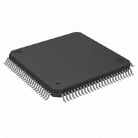
IC MPU 32BIT 25MHZ 100-QFP
Manufacturer
Freescale Semiconductor
Datasheet
1.MC68EC020AA16.pdf
(306 pages)
Specifications of MC68EC020AA25
Processor Type
M680x0 32-Bit
Speed
25MHz
Voltage
5V
Mounting Type
Surface Mount
Package / Case
100-QFP
Family Name
M68000
Device Core
ColdFire
Device Core Size
32b
Frequency (max)
25MHz
Instruction Set Architecture
RISC
Supply Voltage 1 (typ)
5V
Operating Supply Voltage (max)
5.25V
Operating Supply Voltage (min)
4.75V
Operating Temp Range
0C to 70C
Operating Temperature Classification
Commercial
Mounting
Surface Mount
Pin Count
100
Package Type
PQFP
Lead Free Status / RoHS Status
Lead free / RoHS Compliant
Features
-
Lead Free Status / Rohs Status
RoHS Compliant part
Electrostatic Device
Available stocks
Company
Part Number
Manufacturer
Quantity
Price
Company:

Part Number:
MC68EC020AA25
Manufacturer:
Freescale Semiconductor
Quantity:
10 000
Company:
Part Number:
MC68EC020AA25R
Manufacturer:
Freescale Semiconductor
Quantity:
10 000


State 4
State 5
5-32
MC68020/EC020—At the end of state 4 (S4), the processor latches the incoming data.
MC68020—The processor negates AS, DS, and DBEN during state 5 (S5). It holds the
MC68EC020—The processor negates AS and DS during state S5. It holds the address
address valid during S5 to provide address hold time for memory systems. R/W, SIZ1–
SIZ0, and FC2–FC0 also remain valid throughout S5.
The external device keeps its data and DSACK1/DSACK0 signals asserted until it
detects the negation of AS or DS (whichever it detects first). The device must remove
its data and negate DSACK1/DSACK0 within approximately one clock period after
sensing the negation of AS or DS. DSACK1/DSACK0 signals that remain asserted
beyond this limit may be prematurely detected for the next bus cycle.
valid during S5 to provide address hold time for memory systems. R/W , SIZ1, SIZ0,
and FC2–FC0 also remain valid throughout S5.
The external device keeps its data and DSACK1/DSACK0 signals asserted until it
detects the negation of AS or DS (whichever it detects first). The device must remove
its data and negate DSACK1/DSACK0 within approximately one clock period after
sensing the negation of AS or DS. DSACK1/DSACK0 signals that remain asserted
beyond this limit may be prematurely detected for the next bus cycle.
M68020 USER’S MANUAL
MOTOROLA
Related parts for MC68EC020AA25
Image
Part Number
Description
Manufacturer
Datasheet
Request
R

Part Number:
Description:
Manufacturer:
Freescale Semiconductor, Inc
Datasheet:
Part Number:
Description:
Manufacturer:
Freescale Semiconductor, Inc
Datasheet:
Part Number:
Description:
Manufacturer:
Freescale Semiconductor, Inc
Datasheet:
Part Number:
Description:
Manufacturer:
Freescale Semiconductor, Inc
Datasheet:
Part Number:
Description:
Manufacturer:
Freescale Semiconductor, Inc
Datasheet:
Part Number:
Description:
Manufacturer:
Freescale Semiconductor, Inc
Datasheet:
Part Number:
Description:
Manufacturer:
Freescale Semiconductor, Inc
Datasheet:
Part Number:
Description:
Manufacturer:
Freescale Semiconductor, Inc
Datasheet:
Part Number:
Description:
Manufacturer:
Freescale Semiconductor, Inc
Datasheet:
Part Number:
Description:
Manufacturer:
Freescale Semiconductor, Inc
Datasheet:
Part Number:
Description:
Manufacturer:
Freescale Semiconductor, Inc
Datasheet:
Part Number:
Description:
Manufacturer:
Freescale Semiconductor, Inc
Datasheet:
Part Number:
Description:
Manufacturer:
Freescale Semiconductor, Inc
Datasheet:
Part Number:
Description:
Manufacturer:
Freescale Semiconductor, Inc
Datasheet:
Part Number:
Description:
Manufacturer:
Freescale Semiconductor, Inc
Datasheet: