MC68EC020AA25 Freescale Semiconductor, MC68EC020AA25 Datasheet - Page 123
MC68EC020AA25
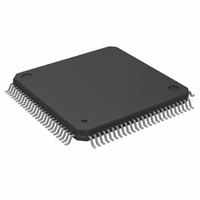
Manufacturer Part Number
MC68EC020AA25
Description
IC MPU 32BIT 25MHZ 100-QFP
Manufacturer
Freescale Semiconductor
Datasheet
1.MC68EC020AA16.pdf
(306 pages)
Specifications of MC68EC020AA25
Processor Type
M680x0 32-Bit
Speed
25MHz
Voltage
5V
Mounting Type
Surface Mount
Package / Case
100-QFP
Family Name
M68000
Device Core
ColdFire
Device Core Size
32b
Frequency (max)
25MHz
Instruction Set Architecture
RISC
Supply Voltage 1 (typ)
5V
Operating Supply Voltage (max)
5.25V
Operating Supply Voltage (min)
4.75V
Operating Temp Range
0C to 70C
Operating Temperature Classification
Commercial
Mounting
Surface Mount
Pin Count
100
Package Type
PQFP
Lead Free Status / RoHS Status
Lead free / RoHS Compliant
Features
-
Lead Free Status / Rohs Status
RoHS Compliant part
Electrostatic Device
Available stocks
Company
Part Number
Manufacturer
Quantity
Price
Company:

Part Number:
MC68EC020AA25
Manufacturer:
Freescale Semiconductor
Quantity:
10 000
Company:
Part Number:
MC68EC020AA25R
Manufacturer:
Freescale Semiconductor
Quantity:
10 000


An example of MC68EC020 bus arbitration to a DMA device that supports three-wire bus
arbitration is described in Appendix A Interfacing an MC68EC020 to a DMA Device
That Supports a Three-Wire Bus Arbitration Protocol.
5.8 RESET OPERATION
RESET is a bidirectional signal with which an external device resets the system or the
processor resets external devices. When power is applied to the system, external circuitry
should assert RESET for a minimum of 520 clocks after V
stabilized and are within specification limits. Figure 5-51 is a timing diagram of the power-
up reset operation, showing the relationships between RESET, V
clock signal is required to be stable by the time V
specification. During the reset period, the entire bus three-states (except for non-three-
statable signals, which are driven to their inactive state). Once RESET negates, all control
signals are negated, the data bus is in read mode, and the address bus is driven. After
this, the first bus cycle for reset exception processing begins.
The external RESET signal resets the processor and the entire system. Except for the
initial reset, RESET should be asserted for at least 520 clock periods to ensure that the
processor resets. Asserting RESET for 10 clock periods is sufficient for resetting the
processor logic; the additional clock periods prevent a RESET instruction from overlapping
the external RESET signal.
5-76
Figure 5-50. Interface for Three-Wire to Two-Wire Bus Arbitration
BUS MASTER
ALTERNATE
BGACK
M68020 USER’S MANUAL
AS
BG
BR
CC
AS
BG
BR
MC68EC020
reaches the minimum operating
CC
CC
and clock timing have
, and bus signals. The
MOTOROLA
Related parts for MC68EC020AA25
Image
Part Number
Description
Manufacturer
Datasheet
Request
R

Part Number:
Description:
Manufacturer:
Freescale Semiconductor, Inc
Datasheet:
Part Number:
Description:
Manufacturer:
Freescale Semiconductor, Inc
Datasheet:
Part Number:
Description:
Manufacturer:
Freescale Semiconductor, Inc
Datasheet:
Part Number:
Description:
Manufacturer:
Freescale Semiconductor, Inc
Datasheet:
Part Number:
Description:
Manufacturer:
Freescale Semiconductor, Inc
Datasheet:
Part Number:
Description:
Manufacturer:
Freescale Semiconductor, Inc
Datasheet:
Part Number:
Description:
Manufacturer:
Freescale Semiconductor, Inc
Datasheet:
Part Number:
Description:
Manufacturer:
Freescale Semiconductor, Inc
Datasheet:
Part Number:
Description:
Manufacturer:
Freescale Semiconductor, Inc
Datasheet:
Part Number:
Description:
Manufacturer:
Freescale Semiconductor, Inc
Datasheet:
Part Number:
Description:
Manufacturer:
Freescale Semiconductor, Inc
Datasheet:
Part Number:
Description:
Manufacturer:
Freescale Semiconductor, Inc
Datasheet:
Part Number:
Description:
Manufacturer:
Freescale Semiconductor, Inc
Datasheet:
Part Number:
Description:
Manufacturer:
Freescale Semiconductor, Inc
Datasheet:
Part Number:
Description:
Manufacturer:
Freescale Semiconductor, Inc
Datasheet: