MC68EC020AA25 Freescale Semiconductor, MC68EC020AA25 Datasheet - Page 121
MC68EC020AA25
Manufacturer Part Number
MC68EC020AA25
Description
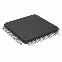
IC MPU 32BIT 25MHZ 100-QFP
Manufacturer
Freescale Semiconductor
Datasheet
1.MC68EC020AA16.pdf
(306 pages)
Specifications of MC68EC020AA25
Processor Type
M680x0 32-Bit
Speed
25MHz
Voltage
5V
Mounting Type
Surface Mount
Package / Case
100-QFP
Family Name
M68000
Device Core
ColdFire
Device Core Size
32b
Frequency (max)
25MHz
Instruction Set Architecture
RISC
Supply Voltage 1 (typ)
5V
Operating Supply Voltage (max)
5.25V
Operating Supply Voltage (min)
4.75V
Operating Temp Range
0C to 70C
Operating Temperature Classification
Commercial
Mounting
Surface Mount
Pin Count
100
Package Type
PQFP
Lead Free Status / RoHS Status
Lead free / RoHS Compliant
Features
-
Lead Free Status / Rohs Status
RoHS Compliant part
Electrostatic Device
Available stocks
Company
Part Number
Manufacturer
Quantity
Price
Company:

Part Number:
MC68EC020AA25
Manufacturer:
Freescale Semiconductor
Quantity:
10 000
Company:
Part Number:
MC68EC020AA25R
Manufacturer:
Freescale Semiconductor
Quantity:
10 000


State changes occur on the next rising edge of the clock after the internal signal is
recognized as valid. The BG signal transitions on the falling edge of the clock after a state
is reached during which G changes. The bus control signals (controlled by T) are driven
by the processor immediately following a state change when bus mastership is returned to
the MC68EC020.
State 0, at the top center of the diagram, in which both G and T are negated, is the state
of the bus arbiter while the processor is bus master. Request R keeps the arbiter in state 0
as long as it is negated. When a request R is received, both grant G and signal T are
asserted (in state 1 at the top left). The next clock causes a change to state 2, at the lower
left, in which G and T are held. The bus arbiter remains in that state until request R is
negated. Then the arbiter changes to the center state, state 3, and negates grant G. The
next clock takes the arbiter to state 4, at the upper right, in which grant G remains negated
and signal T remains asserted. The arbiter returns to the original state, state 0, and
negates signal T. This sequence of states follows the normal sequence of signals for
relinquishing the bus to an external bus master. Other states apply to other possible
sequences of R.
The MC68EC020 does not allow arbitration of the external bus during the read-modify-
write sequence. For the duration of this sequence, the MC68EC020 ignores the BR input.
If mastership of the MC68EC020 bus is required during a read-modify-write operation,
BERR must be used to abort the read-modify-write sequence. The bus arbitration
sequence while the bus is inactive (i.e., executing internal operations such as a multiply
instruction) is shown in Figure 5-49.
5-74
M68020 USER’S MANUAL
MOTOROLA
Related parts for MC68EC020AA25
Image
Part Number
Description
Manufacturer
Datasheet
Request
R

Part Number:
Description:
Manufacturer:
Freescale Semiconductor, Inc
Datasheet:
Part Number:
Description:
Manufacturer:
Freescale Semiconductor, Inc
Datasheet:
Part Number:
Description:
Manufacturer:
Freescale Semiconductor, Inc
Datasheet:
Part Number:
Description:
Manufacturer:
Freescale Semiconductor, Inc
Datasheet:
Part Number:
Description:
Manufacturer:
Freescale Semiconductor, Inc
Datasheet:
Part Number:
Description:
Manufacturer:
Freescale Semiconductor, Inc
Datasheet:
Part Number:
Description:
Manufacturer:
Freescale Semiconductor, Inc
Datasheet:
Part Number:
Description:
Manufacturer:
Freescale Semiconductor, Inc
Datasheet:
Part Number:
Description:
Manufacturer:
Freescale Semiconductor, Inc
Datasheet:
Part Number:
Description:
Manufacturer:
Freescale Semiconductor, Inc
Datasheet:
Part Number:
Description:
Manufacturer:
Freescale Semiconductor, Inc
Datasheet:
Part Number:
Description:
Manufacturer:
Freescale Semiconductor, Inc
Datasheet:
Part Number:
Description:
Manufacturer:
Freescale Semiconductor, Inc
Datasheet:
Part Number:
Description:
Manufacturer:
Freescale Semiconductor, Inc
Datasheet:
Part Number:
Description:
Manufacturer:
Freescale Semiconductor, Inc
Datasheet: