MC68EC020AA25 Freescale Semiconductor, MC68EC020AA25 Datasheet - Page 4
MC68EC020AA25
Manufacturer Part Number
MC68EC020AA25
Description
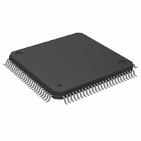
IC MPU 32BIT 25MHZ 100-QFP
Manufacturer
Freescale Semiconductor
Datasheet
1.MC68EC020AA16.pdf
(306 pages)
Specifications of MC68EC020AA25
Processor Type
M680x0 32-Bit
Speed
25MHz
Voltage
5V
Mounting Type
Surface Mount
Package / Case
100-QFP
Family Name
M68000
Device Core
ColdFire
Device Core Size
32b
Frequency (max)
25MHz
Instruction Set Architecture
RISC
Supply Voltage 1 (typ)
5V
Operating Supply Voltage (max)
5.25V
Operating Supply Voltage (min)
4.75V
Operating Temp Range
0C to 70C
Operating Temperature Classification
Commercial
Mounting
Surface Mount
Pin Count
100
Package Type
PQFP
Lead Free Status / RoHS Status
Lead free / RoHS Compliant
Features
-
Lead Free Status / Rohs Status
RoHS Compliant part
Electrostatic Device
Available stocks
Company
Part Number
Manufacturer
Quantity
Price
Company:

Part Number:
MC68EC020AA25
Manufacturer:
Freescale Semiconductor
Quantity:
10 000
Company:
Part Number:
MC68EC020AA25R
Manufacturer:
Freescale Semiconductor
Quantity:
10 000


9/29/95
Paragraph
3.12
3.13
4.1
4.2
4.3
4.3.1
4.3.2
5.1
5.1.1
5.1.2
5.1.3
5.1.4
5.1.5
5.1.6
5.1.7
5.2
5.2.1
5.2.2
5.2.3
5.2.4
5.2.5
5.2.6
5.2.7
5.3
5.3.1
5.3.2
5.3.3
5.4
5.4.1
5.4.1.1
5.4.1.2
5.4.1.3
5.4.2
5.4.3
5.5
5.5.1
viii
Number
Power Supply Connections ..................................................................... 3-7
Signal Summary...................................................................................... 3-8
On-Chip Cache Organization and Operation .......................................... 4-1
Cache Reset ........................................................................................... 4-3
Cache Control ......................................................................................... 4-3
Bus Transfer Signals............................................................................... 5-1
Data Transfer Mechanism....................................................................... 5-5
Data Transfer Cycles .............................................................................. 5-25
CPU Space Cycles ................................................................................. 5-44
Bus Exception Control Cycles................................................................. 5-53
Cache Control Register (CACR) ......................................................... 4-3
Cache Address Register (CAAR) ........................................................ 4-4
Bus Control Signals ............................................................................. 5-2
Address Bus ........................................................................................ 5-3
Data Strobe ......................................................................................... 5-4
Data Buffer Enable .............................................................................. 5-4
Bus Cycle Termination Signals............................................................ 5-4
Dynamic Bus Sizing ............................................................................ 5-5
Misaligned Operands........................................................................... 5-14
Effects of Dynamic Bus Sizing and Operand Misalignment ................ 5-20
Address, Size, and Data Bus Relationships ........................................ 5-21
Cache Interactions .............................................................................. 5-22
Synchronous Operation with DSACK1/DSACK0 ............................... 5-24
Read Cycle .......................................................................................... 5-26
Write Cycle .......................................................................................... 5-33
Read-Modify-Write Cycle..................................................................... 5-39
Interrupt Acknowledge Bus Cycles ...................................................... 5-45
Breakpoint Acknowledge Cycle ........................................................... 5-50
Coprocessor Communication Cycles .................................................. 5-53
Address Strobe .................................................................................... 5-3
Data Bus.............................................................................................. 5-3
Bus Operation ..................................................................................... 5-24
Bus Errors ........................................................................................... 5-55
TABLE OF CONTENTS (Continued)
Interrupt Acknowledge Cycle—Terminated Normally ...................... 5-45
Autovector Interrupt Acknowledge Cycle ......................................... 5-48
Spurious Interrupt Cycle .................................................................. 5-48
SECTION 1: OVERVIEW
On-Chip Cache Memory
M68020 USER’S MANUAL
Bus Operation
Section 4
Section 5
Title
UM Rev.1.0
MOTOROLA
Number
Page
Related parts for MC68EC020AA25
Image
Part Number
Description
Manufacturer
Datasheet
Request
R

Part Number:
Description:
Manufacturer:
Freescale Semiconductor, Inc
Datasheet:
Part Number:
Description:
Manufacturer:
Freescale Semiconductor, Inc
Datasheet:
Part Number:
Description:
Manufacturer:
Freescale Semiconductor, Inc
Datasheet:
Part Number:
Description:
Manufacturer:
Freescale Semiconductor, Inc
Datasheet:
Part Number:
Description:
Manufacturer:
Freescale Semiconductor, Inc
Datasheet:
Part Number:
Description:
Manufacturer:
Freescale Semiconductor, Inc
Datasheet:
Part Number:
Description:
Manufacturer:
Freescale Semiconductor, Inc
Datasheet:
Part Number:
Description:
Manufacturer:
Freescale Semiconductor, Inc
Datasheet:
Part Number:
Description:
Manufacturer:
Freescale Semiconductor, Inc
Datasheet:
Part Number:
Description:
Manufacturer:
Freescale Semiconductor, Inc
Datasheet:
Part Number:
Description:
Manufacturer:
Freescale Semiconductor, Inc
Datasheet:
Part Number:
Description:
Manufacturer:
Freescale Semiconductor, Inc
Datasheet:
Part Number:
Description:
Manufacturer:
Freescale Semiconductor, Inc
Datasheet:
Part Number:
Description:
Manufacturer:
Freescale Semiconductor, Inc
Datasheet:
Part Number:
Description:
Manufacturer:
Freescale Semiconductor, Inc
Datasheet: