MC68EC020AA25 Freescale Semiconductor, MC68EC020AA25 Datasheet - Page 68
MC68EC020AA25
Manufacturer Part Number
MC68EC020AA25
Description
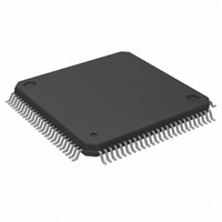
IC MPU 32BIT 25MHZ 100-QFP
Manufacturer
Freescale Semiconductor
Datasheet
1.MC68EC020AA16.pdf
(306 pages)
Specifications of MC68EC020AA25
Processor Type
M680x0 32-Bit
Speed
25MHz
Voltage
5V
Mounting Type
Surface Mount
Package / Case
100-QFP
Family Name
M68000
Device Core
ColdFire
Device Core Size
32b
Frequency (max)
25MHz
Instruction Set Architecture
RISC
Supply Voltage 1 (typ)
5V
Operating Supply Voltage (max)
5.25V
Operating Supply Voltage (min)
4.75V
Operating Temp Range
0C to 70C
Operating Temperature Classification
Commercial
Mounting
Surface Mount
Pin Count
100
Package Type
PQFP
Lead Free Status / RoHS Status
Lead free / RoHS Compliant
Features
-
Lead Free Status / Rohs Status
RoHS Compliant part
Electrostatic Device
Available stocks
Company
Part Number
Manufacturer
Quantity
Price
Company:

Part Number:
MC68EC020AA25
Manufacturer:
Freescale Semiconductor
Quantity:
10 000
Company:
Part Number:
MC68EC020AA25R
Manufacturer:
Freescale Semiconductor
Quantity:
10 000


Table 5-6 demonstrates that the processor always prefetches instructions by reading a
long word from a long-word address (A1, A0 = 00), regardless of port size or alignment.
When the required instruction begins at an odd-word boundary, the processor attempts to
fetch the entire 32 bits and loads both words into the instruction cache, if possible,
although the second one is the required word. Even if the instruction access is not cached,
the entire 32 bits are latched into an internal cache holding register from which the two
instructions words can subsequently be referenced. Refer to Section 8 Instruction
Execution Timing for a complete description of the cache holding register and pipeline
operation.
5.2.4 Address, Size, and Data Bus Relationships
The data transfer examples show how the MC68020/EC020 drives data onto or receives
data from the correct byte sections of the data bus. Table 5-7 shows the combinations of
the SIZ1, SIZ0, A1, and A0 signals that can be used to generate byte enable signals for
each of the four sections of the data bus for read and write cycles if the addressed device
requires them. The port size also affects the generation of these enable signals as shown
in the table. The four columns on the right correspond to the four byte enable signals.
Letters B, W, and L refer to port sizes: B for 8-bit ports, W for 16-bit ports, and L for 32-bit
ports. The letters B, W, and L imply that the byte enable signal should be true for that port
size. A dash (—) implies that the byte enable signal does not apply.
The MC68020/EC020 always drives all sections of the data bus because, at the beginning
of a write cycle, the bus controller does not know the port size.
Table 5-7 reveals that the MC68020/EC020 transfers the number of bytes specified by
SIZ1, SIZ0 to or from the specified address unless the operand is misaligned or unless the
number of bytes is greater than the port width. In these cases, the device transfers the
greatest number of bytes possible for the port. For example, if the size is four and A1, A0
= 01, a 32-bit slave can only receive three bytes in the current bus cycle. A 16- or 8-bit
slave can only receive one byte. The table defines the byte enables for all port sizes. Byte
data strobes can be obtained by combining the enable signals with the DS signal. Devices
residing on 8-bit ports can use the data strobe by itself since there is only one valid byte
for every transfer. These enable or strobe signals select only the bytes required for write
or read cycles. The other bytes are not selected, which prevents incorrect accesses in
sensitive areas such as I/O.
MOTOROLA
M68020 USER’S MANUAL
5- 21
Related parts for MC68EC020AA25
Image
Part Number
Description
Manufacturer
Datasheet
Request
R

Part Number:
Description:
Manufacturer:
Freescale Semiconductor, Inc
Datasheet:
Part Number:
Description:
Manufacturer:
Freescale Semiconductor, Inc
Datasheet:
Part Number:
Description:
Manufacturer:
Freescale Semiconductor, Inc
Datasheet:
Part Number:
Description:
Manufacturer:
Freescale Semiconductor, Inc
Datasheet:
Part Number:
Description:
Manufacturer:
Freescale Semiconductor, Inc
Datasheet:
Part Number:
Description:
Manufacturer:
Freescale Semiconductor, Inc
Datasheet:
Part Number:
Description:
Manufacturer:
Freescale Semiconductor, Inc
Datasheet:
Part Number:
Description:
Manufacturer:
Freescale Semiconductor, Inc
Datasheet:
Part Number:
Description:
Manufacturer:
Freescale Semiconductor, Inc
Datasheet:
Part Number:
Description:
Manufacturer:
Freescale Semiconductor, Inc
Datasheet:
Part Number:
Description:
Manufacturer:
Freescale Semiconductor, Inc
Datasheet:
Part Number:
Description:
Manufacturer:
Freescale Semiconductor, Inc
Datasheet:
Part Number:
Description:
Manufacturer:
Freescale Semiconductor, Inc
Datasheet:
Part Number:
Description:
Manufacturer:
Freescale Semiconductor, Inc
Datasheet:
Part Number:
Description:
Manufacturer:
Freescale Semiconductor, Inc
Datasheet: