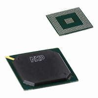
PNX1501E,557 NXP Semiconductors, PNX1501E,557 Datasheet - Page 747

PNX1501E,557
Manufacturer Part Number
PNX1501E,557
Description
IC MEDIA PROC 266MHZ 456-BGA
Manufacturer
NXP Semiconductors
Datasheet
1.PNX1502EG557.pdf
(828 pages)
Specifications of PNX1501E,557
Applications
Multimedia
Core Processor
TriMedia
Controller Series
Nexperia
Interface
I²C, 2-Wire Serial
Number Of I /o
61
Voltage - Supply
1.14 V ~ 1.26 V
Operating Temperature
0°C ~ 85°C
Mounting Type
Surface Mount
Package / Case
456-BGA
Lead Free Status / RoHS Status
Lead free / RoHS Compliant
Program Memory Type
-
Ram Size
-
Other names
935274728557
PNX1501E
PNX1501E
PNX1501E
PNX1501E
Available stocks
Company
Part Number
Manufacturer
Quantity
Price
Company:
Part Number:
PNX1501E,557
Manufacturer:
NXP Semiconductors
Quantity:
10 000
- Current page: 747 of 828
- Download datasheet (8Mb)
1. Introduction
2. Functional Description
2.1.1 Test Access Port (TAP)
1.1 Features
2.1 General Operations
The TM3260 Debug (TM_DBG) interface consists of the Test Access Port (TAP), the
TAP Controller, a JTAG Instruction register and internal debug registers. The TAP
controller from which the TM_DBG module receives its commands resides in the test
control block, which also facilitates boundary scanning and other DFT features.
The TM_DBG has registers that can be programmed for control and communication
with an on-chip TriMedia TM3260 CPU.
The Test Access Port (TAP) includes four dedicated input pins and one output pin:
TCK provides the clock for test logic required by the JTAG standard. TCK is
asynchronous to any system clock. Stored state devices in the JTAG controller will
retain their state indefinitely when TCK is stopped at 0 or 1.
The signal received at TMS is decoded by the TAP controller to control test functions.
The test logic is required to sample TMS at the rising edge of TCK.
Serial test instructions and test data are received at TDI. The TDI signal is required to
be sampled at the rising edge of TCK. When test data is shifted from TDI to TDO, the
data must appear without inversion at TDO after a number of rising and falling edges
of TCK determined by the length of the instruction or test data register selected.
•
•
•
•
Chapter 24: TM3260 Debug
PNX15xx Series Data Book – Volume 1 of 1
Rev. 3 — 17 March 2006
TCK (Test Clock)
TMS (Test Mode Select)
TDI (Test Data In)
TDO (Test Data Out)
Product data sheet
Related parts for PNX1501E,557
Image
Part Number
Description
Manufacturer
Datasheet
Request
R
Part Number:
Description:
Manufacturer:
NXP Semiconductors
Datasheet:
Part Number:
Description:
Digital Signal Processors & Controllers (DSP, DSC) MEDIA PROCESSOR PNX15XX/266MHZ
Manufacturer:
NXP Semiconductors
Datasheet:

Part Number:
Description:
IC MEDIA PROC 266MHZ 456-BGA
Manufacturer:
NXP Semiconductors
Datasheet:
Part Number:
Description:
NXP Semiconductors designed the LPC2420/2460 microcontroller around a 16-bit/32-bitARM7TDMI-S CPU core with real-time debug interfaces that include both JTAG andembedded trace
Manufacturer:
NXP Semiconductors
Datasheet:

Part Number:
Description:
NXP Semiconductors designed the LPC2458 microcontroller around a 16-bit/32-bitARM7TDMI-S CPU core with real-time debug interfaces that include both JTAG andembedded trace
Manufacturer:
NXP Semiconductors
Datasheet:
Part Number:
Description:
NXP Semiconductors designed the LPC2468 microcontroller around a 16-bit/32-bitARM7TDMI-S CPU core with real-time debug interfaces that include both JTAG andembedded trace
Manufacturer:
NXP Semiconductors
Datasheet:
Part Number:
Description:
NXP Semiconductors designed the LPC2470 microcontroller, powered by theARM7TDMI-S core, to be a highly integrated microcontroller for a wide range ofapplications that require advanced communications and high quality graphic displays
Manufacturer:
NXP Semiconductors
Datasheet:
Part Number:
Description:
NXP Semiconductors designed the LPC2478 microcontroller, powered by theARM7TDMI-S core, to be a highly integrated microcontroller for a wide range ofapplications that require advanced communications and high quality graphic displays
Manufacturer:
NXP Semiconductors
Datasheet:
Part Number:
Description:
The Philips Semiconductors XA (eXtended Architecture) family of 16-bit single-chip microcontrollers is powerful enough to easily handle the requirements of high performance embedded applications, yet inexpensive enough to compete in the market for hi
Manufacturer:
NXP Semiconductors
Datasheet:
Part Number:
Description:
The XA-S3 device is a member of Philips Semiconductors? XA(eXtended Architecture) family of high performance 16-bitsingle-chip microcontrollers
Manufacturer:
NXP Semiconductors
Datasheet:

Part Number:
Description:
The NXP BlueStreak LH75401/LH75411 family consists of two low-cost 16/32-bit System-on-Chip (SoC) devices
Manufacturer:
NXP Semiconductors
Datasheet:

Part Number:
Description:
The NXP LPC3130/3131 combine an 180 MHz ARM926EJ-S CPU core, high-speed USB2
Manufacturer:
NXP Semiconductors
Datasheet:

Part Number:
Description:
The NXP LPC3141 combine a 270 MHz ARM926EJ-S CPU core, High-speed USB 2
Manufacturer:
NXP Semiconductors

Part Number:
Description:
The NXP LPC3143 combine a 270 MHz ARM926EJ-S CPU core, High-speed USB 2
Manufacturer:
NXP Semiconductors


