PNX1501E,557 NXP Semiconductors, PNX1501E,557 Datasheet - Page 342
PNX1501E,557
Manufacturer Part Number
PNX1501E,557
Description
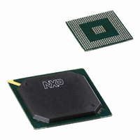
IC MEDIA PROC 266MHZ 456-BGA
Manufacturer
NXP Semiconductors
Datasheet
1.PNX1502EG557.pdf
(828 pages)
Specifications of PNX1501E,557
Applications
Multimedia
Core Processor
TriMedia
Controller Series
Nexperia
Interface
I²C, 2-Wire Serial
Number Of I /o
61
Voltage - Supply
1.14 V ~ 1.26 V
Operating Temperature
0°C ~ 85°C
Mounting Type
Surface Mount
Package / Case
456-BGA
Lead Free Status / RoHS Status
Lead free / RoHS Compliant
Program Memory Type
-
Ram Size
-
Other names
935274728557
PNX1501E
PNX1501E
PNX1501E
PNX1501E
Available stocks
Company
Part Number
Manufacturer
Quantity
Price
Company:

Part Number:
PNX1501E,557
Manufacturer:
NXP Semiconductors
Quantity:
10 000


Philips Semiconductors
Volume 1 of 1
Table 9: Register Description
PNX15XX_SER_3
Product data sheet
Bit
Offset 0x06 5120
31:4
3:0
Offset 0x06 5124
31:4
3:0
Offset 0x06 5128
31:4
3:0
Offset 0x06 512C
31:6
15:0
Arbitration Parameters
Offset 0x06 5180
31
30
29
28
27:18
Symbol
Unused
TRFC
Unused
TMRD
Unused
TCAS
Unused
RF_PERIOD
CPU_DMA_DECR
CPU_HRT_SRT_ENAB
LE
BLB_ENABLE
DYN_RATIOS
Reserved
DDR_TRFC
DDR_TMRD
DDR_TCAS
DDR_RF_PERIOD
ARB_CTL
Access Value
R
R/W
R
R/W
R
R/W
R
R/W
R/W
R/W
R/W
R/W
R
-
0xf
-
2
-
8
-
3515
1
0
0
0
-
Rev. 3 — 17 March 2006
Description
These bits should be ignored when read, and written as 0’s.
Auto refresh command period.
These bits should be ignored when read, and written as 0’s.
Load mode register command cycle time.
These bits should be ignored when read, and written as 0s.
CAS read latency, specified in halve cycles. I.e., a value of 0b0111
(7) represents a CAS delay of 3.5 cycles (7 halve cycles).
These bits should be ignored when read, and written as 0s.
Refresh period expressed in terms of cycles. Typically a refresh is
required at an average interval of 15.625 us. For a 100 MHz. device
this translates into a RF_PERIOD value of 1562. For a 200 MHz.
device this translates into a RF_PERIOD value of 3125.
‘0’: Do not decrement CPU counters when in a DMA_WINDOW.
‘1’: Do decrement CPU counters when in a DMA_WINDOW.
‘0’: Controller will interpret that DMA port contains only Hard Real
Time DMA requests.
‘1’: Controller will interpret that DMA port contains Hard Real Time
or Soft Real Time DMA requests.
‘0’: Disable Back Log Buffer
‘1’: Enable Back Log Buffer.
‘0’: Use Static Ratios. This means accounts are incremented by the
value (RATIO+ DDR burst size (in terms of cycles)) whenever a
CPU DDR burst is performed.
‘1’: Enable Dynamic Ratios. This means accounts are incremented
by the value RATIO every clock cycle that is spent on servicing a
CPU DDR burst. This feature also causes account not to decrement
during clock cycles that are spent on CPU DDR bursts.
These bits should be ignored when read, and written as 0s.
© Koninklijke Philips Electronics N.V. 2006. All rights reserved.
Chapter 9: DDR Controller
PNX15xx Series
9-29
Related parts for PNX1501E,557
Image
Part Number
Description
Manufacturer
Datasheet
Request
R

Part Number:
Description:
Manufacturer:
NXP Semiconductors
Datasheet:
Part Number:
Description:
Digital Signal Processors & Controllers (DSP, DSC) MEDIA PROCESSOR PNX15XX/266MHZ
Manufacturer:
NXP Semiconductors
Datasheet:

Part Number:
Description:
IC MEDIA PROC 266MHZ 456-BGA
Manufacturer:
NXP Semiconductors
Datasheet:
Part Number:
Description:
NXP Semiconductors designed the LPC2420/2460 microcontroller around a 16-bit/32-bitARM7TDMI-S CPU core with real-time debug interfaces that include both JTAG andembedded trace
Manufacturer:
NXP Semiconductors
Datasheet:

Part Number:
Description:
NXP Semiconductors designed the LPC2458 microcontroller around a 16-bit/32-bitARM7TDMI-S CPU core with real-time debug interfaces that include both JTAG andembedded trace
Manufacturer:
NXP Semiconductors
Datasheet:
Part Number:
Description:
NXP Semiconductors designed the LPC2468 microcontroller around a 16-bit/32-bitARM7TDMI-S CPU core with real-time debug interfaces that include both JTAG andembedded trace
Manufacturer:
NXP Semiconductors
Datasheet:
Part Number:
Description:
NXP Semiconductors designed the LPC2470 microcontroller, powered by theARM7TDMI-S core, to be a highly integrated microcontroller for a wide range ofapplications that require advanced communications and high quality graphic displays
Manufacturer:
NXP Semiconductors
Datasheet:
Part Number:
Description:
NXP Semiconductors designed the LPC2478 microcontroller, powered by theARM7TDMI-S core, to be a highly integrated microcontroller for a wide range ofapplications that require advanced communications and high quality graphic displays
Manufacturer:
NXP Semiconductors
Datasheet:
Part Number:
Description:
The Philips Semiconductors XA (eXtended Architecture) family of 16-bit single-chip microcontrollers is powerful enough to easily handle the requirements of high performance embedded applications, yet inexpensive enough to compete in the market for hi
Manufacturer:
NXP Semiconductors
Datasheet:
Part Number:
Description:
The XA-S3 device is a member of Philips Semiconductors? XA(eXtended Architecture) family of high performance 16-bitsingle-chip microcontrollers
Manufacturer:
NXP Semiconductors
Datasheet:

Part Number:
Description:
The NXP BlueStreak LH75401/LH75411 family consists of two low-cost 16/32-bit System-on-Chip (SoC) devices
Manufacturer:
NXP Semiconductors
Datasheet:
Part Number:
Description:
The NXP LPC3130/3131 combine an 180 MHz ARM926EJ-S CPU core, high-speed USB2
Manufacturer:
NXP Semiconductors
Datasheet:
Part Number:
Description:
The NXP LPC3141 combine a 270 MHz ARM926EJ-S CPU core, High-speed USB 2
Manufacturer:
NXP Semiconductors
Part Number:
Description:
The NXP LPC3143 combine a 270 MHz ARM926EJ-S CPU core, High-speed USB 2
Manufacturer:
NXP Semiconductors