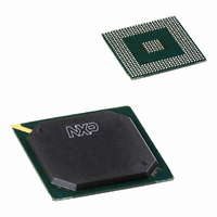
PNX1501E,557 NXP Semiconductors, PNX1501E,557 Datasheet - Page 29

PNX1501E,557
Manufacturer Part Number
PNX1501E,557
Description
IC MEDIA PROC 266MHZ 456-BGA
Manufacturer
NXP Semiconductors
Datasheet
1.PNX1502EG557.pdf
(828 pages)
Specifications of PNX1501E,557
Applications
Multimedia
Core Processor
TriMedia
Controller Series
Nexperia
Interface
I²C, 2-Wire Serial
Number Of I /o
61
Voltage - Supply
1.14 V ~ 1.26 V
Operating Temperature
0°C ~ 85°C
Mounting Type
Surface Mount
Package / Case
456-BGA
Lead Free Status / RoHS Status
Lead free / RoHS Compliant
Program Memory Type
-
Ram Size
-
Other names
935274728557
PNX1501E
PNX1501E
PNX1501E
PNX1501E
Available stocks
Company
Part Number
Manufacturer
Quantity
Price
Company:
Part Number:
PNX1501E,557
Manufacturer:
NXP Semiconductors
Quantity:
10 000
- Current page: 29 of 828
- Download datasheet (8Mb)
Philips Semiconductors
Volume 1 of 1
Table 1: PNX1500 I/O Types
Table 2: PNX1500 I/O Modes
PNX15XX_SER_3
Product data sheet
Pad Type
PCIT5V
IIC3M4SDAT5V
IIC3M4SCLT5V
BPX2T14MCP
BPTS1CP
BPTS1CHP
BPTS3CP
BPTS3CHP
BPT3MCHT5V
BPT3MCHDT5V 3.3-V regular impedance output, with slow rise/fall time, combined with 5-V tolerant input with hysteresis
IPCP
IPCHP
SSTLCLKIO
SSTLADDIO
SSTLDATIO
Modes
IN
OUT
OD
I/O
I/OD
I/O/D
O
Description
PCI 2.2 compliant I/O using 3.3- or 5- V PCI signaling conventions.
Open drain 3.3- or 5- V I
3.3-V low impedance output, with fast rise/fall time, combined with 3.3-V input only.
Used for Clock signals requires board level 27-33
3.3-V regular impedance output, with fast rise/fall time, combined with 3.3-V input only.
3.3-V regular impedance output, with fast rise/fall time, combined with 3.3-V input only with hysteresis.
3.3-V regular impedance output, with slow rise/fall time, combined with 3.3-V input only.
3.3-V regular impedance output, with slow rise/fall time, combined with 3.3-V input only with hysteresis.
3.3-V regular impedance output, with slow rise/fall time, combined with 5-V tolerant input with hysteresis.
and internal pull-down.
Note: The pull-down is NOT strong enough to actually pull down a 5-V TTL input. Instead the TTL input
pin sees a ‘1’.
3.3-V input only.
3.3-V input only with hysteresis.
SSTL_2 low impedance, e.g. DDR SDRAM clocks. Requires a board level 10
to match a 50
SSTL_2 low impedance for output signals, e.g. DDR SDRAM address and control signals. Requires a
board level matched 50
SSTL_2 low impedance for DDR SDRAM data signals. Requires a board level matched 50
Description
Input only, except during boundary scan or GPIO mode.
Output only, except when used as a GPIO pin.
Open drain output - active pull low, no active drive high, requires external pull-up.
Input or Output.
Input or open drain output - active pull low, no active drive high, requires external pull-up.
Input or output or open drain output with input - active pull low, no active drive high, requires external pull-
up when operated in open drain mode.
Output or floating.
PNX1500 uses different I/Os depending on the type of the interface, e.g. PCI, or
electrical characteristics needed for the functionality, e.g. a clock signal requires
sharper edges than a regular signal. The following table summarizes the types of I/
Os, a.k.a. pads, used in PNX1500.
The above pad types are used in the modes listed in the following table
Unused pins may remain unconnected, i.e. floating if they contain an internal pull-up
or pull-down. More specifically,
PCB trace.
2
C I/Os.
PCB trace.
Rev. 3 — 17 March 2006
series terminator resistor to match 50
Chapter 1: Integrated Circuit Data
© Koninklijke Philips Electronics N.V. 2006. All rights reserved.
PNX15xx Series
series terminator resistor
PCB trace.
PCB trace.
1-2
Related parts for PNX1501E,557
Image
Part Number
Description
Manufacturer
Datasheet
Request
R
Part Number:
Description:
Manufacturer:
NXP Semiconductors
Datasheet:
Part Number:
Description:
Digital Signal Processors & Controllers (DSP, DSC) MEDIA PROCESSOR PNX15XX/266MHZ
Manufacturer:
NXP Semiconductors
Datasheet:

Part Number:
Description:
IC MEDIA PROC 266MHZ 456-BGA
Manufacturer:
NXP Semiconductors
Datasheet:
Part Number:
Description:
NXP Semiconductors designed the LPC2420/2460 microcontroller around a 16-bit/32-bitARM7TDMI-S CPU core with real-time debug interfaces that include both JTAG andembedded trace
Manufacturer:
NXP Semiconductors
Datasheet:

Part Number:
Description:
NXP Semiconductors designed the LPC2458 microcontroller around a 16-bit/32-bitARM7TDMI-S CPU core with real-time debug interfaces that include both JTAG andembedded trace
Manufacturer:
NXP Semiconductors
Datasheet:
Part Number:
Description:
NXP Semiconductors designed the LPC2468 microcontroller around a 16-bit/32-bitARM7TDMI-S CPU core with real-time debug interfaces that include both JTAG andembedded trace
Manufacturer:
NXP Semiconductors
Datasheet:
Part Number:
Description:
NXP Semiconductors designed the LPC2470 microcontroller, powered by theARM7TDMI-S core, to be a highly integrated microcontroller for a wide range ofapplications that require advanced communications and high quality graphic displays
Manufacturer:
NXP Semiconductors
Datasheet:
Part Number:
Description:
NXP Semiconductors designed the LPC2478 microcontroller, powered by theARM7TDMI-S core, to be a highly integrated microcontroller for a wide range ofapplications that require advanced communications and high quality graphic displays
Manufacturer:
NXP Semiconductors
Datasheet:
Part Number:
Description:
The Philips Semiconductors XA (eXtended Architecture) family of 16-bit single-chip microcontrollers is powerful enough to easily handle the requirements of high performance embedded applications, yet inexpensive enough to compete in the market for hi
Manufacturer:
NXP Semiconductors
Datasheet:
Part Number:
Description:
The XA-S3 device is a member of Philips Semiconductors? XA(eXtended Architecture) family of high performance 16-bitsingle-chip microcontrollers
Manufacturer:
NXP Semiconductors
Datasheet:

Part Number:
Description:
The NXP BlueStreak LH75401/LH75411 family consists of two low-cost 16/32-bit System-on-Chip (SoC) devices
Manufacturer:
NXP Semiconductors
Datasheet:

Part Number:
Description:
The NXP LPC3130/3131 combine an 180 MHz ARM926EJ-S CPU core, high-speed USB2
Manufacturer:
NXP Semiconductors
Datasheet:

Part Number:
Description:
The NXP LPC3141 combine a 270 MHz ARM926EJ-S CPU core, High-speed USB 2
Manufacturer:
NXP Semiconductors

Part Number:
Description:
The NXP LPC3143 combine a 270 MHz ARM926EJ-S CPU core, High-speed USB 2
Manufacturer:
NXP Semiconductors


