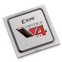
XC4VFX60-10FFG1152C Xilinx Inc, XC4VFX60-10FFG1152C Datasheet - Page 366

XC4VFX60-10FFG1152C
Manufacturer Part Number
XC4VFX60-10FFG1152C
Description
IC FPGA VIRTEX-4 FX 60K 1152FBGA
Manufacturer
Xilinx Inc
Series
Virtex™-4r
Datasheets
1.XC4VFX12-10FFG668C.pdf
(58 pages)
2.XC4VFX12-10FFG668C.pdf
(9 pages)
3.XC4VFX12-10FFG668C.pdf
(406 pages)
Specifications of XC4VFX60-10FFG1152C
Total Ram Bits
4276224
Number Of Logic Elements/cells
56880
Number Of Labs/clbs
6320
Number Of I /o
576
Voltage - Supply
1.14 V ~ 1.26 V
Mounting Type
Surface Mount
Operating Temperature
0°C ~ 85°C
Package / Case
1152-BBGA, FCBGA
No. Of Logic Blocks
6656
No. Of Macrocells
56880
Family Type
Virtex-4
No. Of Speed Grades
10
No. Of I/o's
576
Clock Management
DCM
Core Supply
RoHS Compliant
Package
1152FCBGA
Family Name
Virtex®-4
Device Logic Units
56880
Typical Operating Supply Voltage
1.2 V
Maximum Number Of User I/os
576
Ram Bits
4276224
Lead Free Status / RoHS Status
Lead free / RoHS Compliant
For Use With
HW-V4-ML410-UNI-G - EVALUATION PLATFORM VIRTEX-4
Number Of Gates
-
Lead Free Status / RoHS Status
Lead free / RoHS Compliant
Available stocks
Company
Part Number
Manufacturer
Quantity
Price
Company:
Part Number:
XC4VFX60-10FFG1152C
Manufacturer:
XilinxInc
Quantity:
3 000
Company:
Part Number:
XC4VFX60-10FFG1152C
Manufacturer:
Xilinx Inc
Quantity:
10 000
- XC4VFX12-10FFG668C PDF datasheet
- XC4VFX12-10FFG668C PDF datasheet #2
- XC4VFX12-10FFG668C PDF datasheet #3
- Current page: 366 of 406
- Download datasheet (6Mb)
Chapter 8: Advanced SelectIO Logic Resources
366
•
•
•
Figure 8-1
components and features of the block.
DLYRST
CLKDIV
DLYINC
DLYCE
OCLK
Bitslip
c.
The section
Bitslip Submodule
The Bitslip submodule allows designers to reorder the sequence of the parallel data
stream going into the FPGA logic. This can be used for training source-synchronous
interfaces that include a training pattern.
Dedicated Support for Strobe-based Memory Interfaces
ISERDES contains dedicated circuitry (including the OCLK input pin) to handle the
strobe-to-FPGA clock domain crossover entirely within the ISERDES block. This
allows for higher performance and a simplified implementation.
Dedicated support for Networking interfaces.
REV
CE1
CE2
CLK
SR
D
VARIABLE – Delay value can be changed at run-time by manipulating a set of
control signals
shows the block diagram of the ISERDES, highlighting all the major
“Input Delay Element (IDELAY)” in Chapter 7
IDELAY
Module
Figure 8-1: ISERDES Block Diagram
www.xilinx.com
CE
Serial to Parallel
Converter
BITSLIP
Module
UG070 (v2.6) December 1, 2008
discusses IDELAY in detail.
Virtex-4 FPGA User Guide
O
SHIFTIN1/2
SHIFTOUT1/2
Q1 - Q6
UG70_8_01_031208
R
Related parts for XC4VFX60-10FFG1152C
Image
Part Number
Description
Manufacturer
Datasheet
Request
R

Part Number:
Description:
IC FPGA VIRTEX-4 FX 60K 672-FBGA
Manufacturer:
Xilinx Inc

Part Number:
Description:
IC FPGA VIRTEX-4 FX 60K 672-FBGA
Manufacturer:
Xilinx Inc
Datasheet:

Part Number:
Description:
IC FPGA VIRTEX-4 FX 60K 672-FBGA
Manufacturer:
Xilinx Inc
Datasheet:

Part Number:
Description:
IC FPGA VIRTEX-4 FX 60K 1152FBGA
Manufacturer:
Xilinx Inc
Datasheet:

Part Number:
Description:
IC FPGA VIRTEX-4 FX 60K 1152FBGA
Manufacturer:
Xilinx Inc
Datasheet:

Part Number:
Description:
IC FPGA VIRTEX-4FX 1152FFBGA
Manufacturer:
Xilinx Inc
Datasheet:

Part Number:
Description:
IC FPGA VIRTEX-4FX 1152FFBGA
Manufacturer:
Xilinx Inc
Datasheet:

Part Number:
Description:
FPGA Virtex®-4 Family 56880 Cells 90nm (CMOS) Technology 1.2V 672-Pin FCBGA
Manufacturer:
Xilinx Inc
Datasheet:

Part Number:
Description:
IC FPGA VIRTEX-4 FX 60K 672-FBGA
Manufacturer:
Xilinx Inc
Datasheet:

Part Number:
Description:
IC FPGA VIRTEX-4 FX 60K 672-FBGA
Manufacturer:
Xilinx Inc
Datasheet:

Part Number:
Description:
IC FPGA VIRTEX-4 FX 60K 1152FBGA
Manufacturer:
Xilinx Inc
Datasheet:

Part Number:
Description:
FPGA Virtex®-4 Family 56880 Cells 90nm (CMOS) Technology 1.2V 672-Pin FCBGA
Manufacturer:
Xilinx Inc
Datasheet:

Part Number:
Description:
IC CPLD .8K 36MCELL 44-VQFP
Manufacturer:
Xilinx Inc
Datasheet:

Part Number:
Description:
IC CPLD 72MCRCELL 10NS 44VQFP
Manufacturer:
Xilinx Inc
Datasheet:


