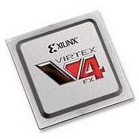
XC4VFX60-10FFG1152C Xilinx Inc, XC4VFX60-10FFG1152C Datasheet - Page 236

XC4VFX60-10FFG1152C
Manufacturer Part Number
XC4VFX60-10FFG1152C
Description
IC FPGA VIRTEX-4 FX 60K 1152FBGA
Manufacturer
Xilinx Inc
Series
Virtex™-4r
Datasheets
1.XC4VFX12-10FFG668C.pdf
(58 pages)
2.XC4VFX12-10FFG668C.pdf
(9 pages)
3.XC4VFX12-10FFG668C.pdf
(406 pages)
Specifications of XC4VFX60-10FFG1152C
Total Ram Bits
4276224
Number Of Logic Elements/cells
56880
Number Of Labs/clbs
6320
Number Of I /o
576
Voltage - Supply
1.14 V ~ 1.26 V
Mounting Type
Surface Mount
Operating Temperature
0°C ~ 85°C
Package / Case
1152-BBGA, FCBGA
No. Of Logic Blocks
6656
No. Of Macrocells
56880
Family Type
Virtex-4
No. Of Speed Grades
10
No. Of I/o's
576
Clock Management
DCM
Core Supply
RoHS Compliant
Package
1152FCBGA
Family Name
Virtex®-4
Device Logic Units
56880
Typical Operating Supply Voltage
1.2 V
Maximum Number Of User I/os
576
Ram Bits
4276224
Lead Free Status / RoHS Status
Lead free / RoHS Compliant
For Use With
HW-V4-ML410-UNI-G - EVALUATION PLATFORM VIRTEX-4
Number Of Gates
-
Lead Free Status / RoHS Status
Lead free / RoHS Compliant
Available stocks
Company
Part Number
Manufacturer
Quantity
Price
Company:
Part Number:
XC4VFX60-10FFG1152C
Manufacturer:
XilinxInc
Quantity:
3 000
Company:
Part Number:
XC4VFX60-10FFG1152C
Manufacturer:
Xilinx Inc
Quantity:
10 000
- XC4VFX12-10FFG668C PDF datasheet
- XC4VFX12-10FFG668C PDF datasheet #2
- XC4VFX12-10FFG668C PDF datasheet #3
- Current page: 236 of 406
- Download datasheet (6Mb)
Chapter 6: SelectIO Resources
236
Virtex-4 FPGA Digitally Controlled Impedance (DCI)
Introduction
Xilinx DCI
As FPGAs get bigger and system clock speeds get faster, PC board design and
manufacturing becomes more difficult. With ever faster edge rates, maintaining signal
integrity becomes a critical issue. PC board traces must be properly terminated to avoid
reflections or ringing.
To terminate a trace, resistors are traditionally added to make the output and/or input
match the impedance of the receiver or driver to the impedance of the trace. However, due
to increased device I/Os, adding resistors close to the device pins increases the board area
and component count, and can in some cases be physically impossible. To address these
issues and to achieve better signal integrity, Xilinx developed the Digitally Controlled
Impedance (DCI) technology.
DCI adjusts the output impedance or input termination to accurately match the
characteristic impedance of the transmission line. DCI actively adjusts the impedance of
the I/O to equal an external reference resistance. This compensates for changes in I/O
impedance due to process variation. It also continuously adjusts the impedance of the I/O
to compensate for variations of temperature and supply voltage fluctuations.
In the case of controlled impedance drivers, DCI controls the driver impedance to match
two reference resistors, or optionally, to match half the value of these reference resistors.
DCI eliminates the need for external series termination resistors.
DCI provides the parallel or series termination for transmitters or receivers. This
eliminates the need for termination resistors on the board, reduces board routing
difficulties and component count, and improves signal integrity by eliminating stub
reflection. Stub reflection occurs when termination resistors are located too far from the
end of the transmission line. With DCI, the termination resistors are as close as possible to
the output driver or the input buffer, thus, eliminating stub reflections.
DCI uses two multi-purpose reference pins in each bank to control the impedance of the
driver or the parallel termination value for all of the I/Os of that bank. The N reference pin
(VRN) must be pulled up to V
must be pulled down to ground by another reference resistor. The value of each reference
resistor should be equal to the characteristic impedance of the PC board traces, or should
be twice that value (see section
page
When a DCI I/O standard is used on a particular bank, the two multi-purpose reference
pins cannot be used as regular I/Os. However, if DCI I/O standards are not used in the
bank, these pins are available as regular I/O pins. The
Specification
DCI adjusts the impedance of the I/O by selectively turning transistors in the I/Os on or
off. The impedance is adjusted to match the external reference resistors. The impedance
adjustment process has two phases. The first phase compensates for process variations by
controlling the larger transistors in the I/Os. It occurs during the device startup sequence.
The second phase maintains the impedance in response to temperature and supply voltage
changes by controlling the smaller transistors in the I/Os. It begins immediately after the
first phase and continues indefinitely, even while the device is operating. By default, the
DONE pin does not go High until the first phase of the impedance adjustment process is
complete.
241).
gives detailed pin descriptions.
www.xilinx.com
CCO
“Driver with Termination to VCCO/2 (Split Termination),”
by a reference resistor, and the P reference pin (VRP)
Virtex-4 Packaging and Pinout
UG070 (v2.6) December 1, 2008
Virtex-4 FPGA User Guide
R
Related parts for XC4VFX60-10FFG1152C
Image
Part Number
Description
Manufacturer
Datasheet
Request
R

Part Number:
Description:
IC FPGA VIRTEX-4 FX 60K 672-FBGA
Manufacturer:
Xilinx Inc

Part Number:
Description:
IC FPGA VIRTEX-4 FX 60K 672-FBGA
Manufacturer:
Xilinx Inc
Datasheet:

Part Number:
Description:
IC FPGA VIRTEX-4 FX 60K 672-FBGA
Manufacturer:
Xilinx Inc
Datasheet:

Part Number:
Description:
IC FPGA VIRTEX-4 FX 60K 1152FBGA
Manufacturer:
Xilinx Inc
Datasheet:

Part Number:
Description:
IC FPGA VIRTEX-4 FX 60K 1152FBGA
Manufacturer:
Xilinx Inc
Datasheet:

Part Number:
Description:
IC FPGA VIRTEX-4FX 1152FFBGA
Manufacturer:
Xilinx Inc
Datasheet:

Part Number:
Description:
IC FPGA VIRTEX-4FX 1152FFBGA
Manufacturer:
Xilinx Inc
Datasheet:

Part Number:
Description:
FPGA Virtex®-4 Family 56880 Cells 90nm (CMOS) Technology 1.2V 672-Pin FCBGA
Manufacturer:
Xilinx Inc
Datasheet:

Part Number:
Description:
IC FPGA VIRTEX-4 FX 60K 672-FBGA
Manufacturer:
Xilinx Inc
Datasheet:

Part Number:
Description:
IC FPGA VIRTEX-4 FX 60K 672-FBGA
Manufacturer:
Xilinx Inc
Datasheet:

Part Number:
Description:
IC FPGA VIRTEX-4 FX 60K 1152FBGA
Manufacturer:
Xilinx Inc
Datasheet:

Part Number:
Description:
FPGA Virtex®-4 Family 56880 Cells 90nm (CMOS) Technology 1.2V 672-Pin FCBGA
Manufacturer:
Xilinx Inc
Datasheet:

Part Number:
Description:
IC CPLD .8K 36MCELL 44-VQFP
Manufacturer:
Xilinx Inc
Datasheet:

Part Number:
Description:
IC CPLD 72MCRCELL 10NS 44VQFP
Manufacturer:
Xilinx Inc
Datasheet:


