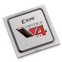
XC4VFX60-10FFG1152C Xilinx Inc, XC4VFX60-10FFG1152C Datasheet - Page 213

XC4VFX60-10FFG1152C
Manufacturer Part Number
XC4VFX60-10FFG1152C
Description
IC FPGA VIRTEX-4 FX 60K 1152FBGA
Manufacturer
Xilinx Inc
Series
Virtex™-4r
Datasheets
1.XC4VFX12-10FFG668C.pdf
(58 pages)
2.XC4VFX12-10FFG668C.pdf
(9 pages)
3.XC4VFX12-10FFG668C.pdf
(406 pages)
Specifications of XC4VFX60-10FFG1152C
Total Ram Bits
4276224
Number Of Logic Elements/cells
56880
Number Of Labs/clbs
6320
Number Of I /o
576
Voltage - Supply
1.14 V ~ 1.26 V
Mounting Type
Surface Mount
Operating Temperature
0°C ~ 85°C
Package / Case
1152-BBGA, FCBGA
No. Of Logic Blocks
6656
No. Of Macrocells
56880
Family Type
Virtex-4
No. Of Speed Grades
10
No. Of I/o's
576
Clock Management
DCM
Core Supply
RoHS Compliant
Package
1152FCBGA
Family Name
Virtex®-4
Device Logic Units
56880
Typical Operating Supply Voltage
1.2 V
Maximum Number Of User I/os
576
Ram Bits
4276224
Lead Free Status / RoHS Status
Lead free / RoHS Compliant
For Use With
HW-V4-ML410-UNI-G - EVALUATION PLATFORM VIRTEX-4
Number Of Gates
-
Lead Free Status / RoHS Status
Lead free / RoHS Compliant
Available stocks
Company
Part Number
Manufacturer
Quantity
Price
Company:
Part Number:
XC4VFX60-10FFG1152C
Manufacturer:
XilinxInc
Quantity:
3 000
Company:
Part Number:
XC4VFX60-10FFG1152C
Manufacturer:
Xilinx Inc
Quantity:
10 000
- XC4VFX12-10FFG668C PDF datasheet
- XC4VFX12-10FFG668C PDF datasheet #2
- XC4VFX12-10FFG668C PDF datasheet #3
- Current page: 213 of 406
- Download datasheet (6Mb)
Virtex-4 FPGA User Guide
UG070 (v2.6) December 1, 2008
Slice Carry-Chain Timing Model and Parameters
R
Clock Event 1: Shift_In
During a Write (Shift_In) operation, the single-bit content of the register at the address on
the ADDR inputs is changed, as data is shifted through the SRL. The data written to this
register is reflected on the X/Y outputs synchronously, if the address is unchanged during
the clock event. If the ADDR inputs are changed during a clock event, the value of the data
at the addressable output (D) is invalid.
•
•
Clock Event 2: Shift_In
•
Clock Event 3: Shift_In/Addressable (Asynchronous) READ
All Read operations are asynchronous to the CLK signal. If the address is changed
(between clock events), the contents of the register at that address are reflected at the
addressable output (X/Y outputs) after a delay of length T
a LUT).
•
•
Clock Event 16: MSB (Most Significant Bit) Changes
At time T
0 in this case) on the XB output of the slice via the MC15 output of the LUT (SRL). This is
also applicable for the XMUX, YMUX, XB, YB, C
T
Figure 5-26
FPGA slice have been omitted for clarity. Only the elements relevant to the timing paths
described in this section are shown.
WOSX
At time T
enabling the SRL for the Write operation that follows.
At time T
and is reflected on the X/Y output after a delay of length T
Since the address 0 is specified at clock event 1, the data on the DI input is reflected at
the D output, because it is written to register 0.
At time T
and is reflected on the X/Y output after a delay of length T
Since the address 0 is still specified at clock event 2, the data on the DI input is
reflected at the D output, because it is written to register 0.
At time T
and is reflected on the X/Y output T
The address is changed (from 0 to 2) some time after clock event 3. The value stored in
register 2 at this time is a 0 (in this example, this was the first data shifted in), and it is
reflected on the X/Y output after a delay of length T
, T
REGXB
WOSXB
illustrates a carry-chain in a Virtex-4 FPGA slice. Some elements of the Virtex-4
WSS
DS
DS
DS
, and T
after clock event 16, the first bit shifted into the SRL becomes valid (logical
before clock event 1 the data becomes valid (0) at the DI input of the SRL
before clock event 2, the data becomes valid (1) at the DI input of the SRL
before clock event 3 the data becomes valid (1) at the DI input of the SRL,
before clock event 1, the write-enable signal (SR) becomes valid-High,
WOSYB
www.xilinx.com
after clock event 16.
REG
time after clock event 3.
OUT
, and F5 outputs at time T
ILO
ILO
.
CLB / Slice Timing Models
(propagation delay through
REG
REG
after clock event 1.
after clock event 2.
WOSCO
,
213
Related parts for XC4VFX60-10FFG1152C
Image
Part Number
Description
Manufacturer
Datasheet
Request
R

Part Number:
Description:
IC FPGA VIRTEX-4 FX 60K 672-FBGA
Manufacturer:
Xilinx Inc

Part Number:
Description:
IC FPGA VIRTEX-4 FX 60K 672-FBGA
Manufacturer:
Xilinx Inc
Datasheet:

Part Number:
Description:
IC FPGA VIRTEX-4 FX 60K 672-FBGA
Manufacturer:
Xilinx Inc
Datasheet:

Part Number:
Description:
IC FPGA VIRTEX-4 FX 60K 1152FBGA
Manufacturer:
Xilinx Inc
Datasheet:

Part Number:
Description:
IC FPGA VIRTEX-4 FX 60K 1152FBGA
Manufacturer:
Xilinx Inc
Datasheet:

Part Number:
Description:
IC FPGA VIRTEX-4FX 1152FFBGA
Manufacturer:
Xilinx Inc
Datasheet:

Part Number:
Description:
IC FPGA VIRTEX-4FX 1152FFBGA
Manufacturer:
Xilinx Inc
Datasheet:

Part Number:
Description:
FPGA Virtex®-4 Family 56880 Cells 90nm (CMOS) Technology 1.2V 672-Pin FCBGA
Manufacturer:
Xilinx Inc
Datasheet:

Part Number:
Description:
IC FPGA VIRTEX-4 FX 60K 672-FBGA
Manufacturer:
Xilinx Inc
Datasheet:

Part Number:
Description:
IC FPGA VIRTEX-4 FX 60K 672-FBGA
Manufacturer:
Xilinx Inc
Datasheet:

Part Number:
Description:
IC FPGA VIRTEX-4 FX 60K 1152FBGA
Manufacturer:
Xilinx Inc
Datasheet:

Part Number:
Description:
FPGA Virtex®-4 Family 56880 Cells 90nm (CMOS) Technology 1.2V 672-Pin FCBGA
Manufacturer:
Xilinx Inc
Datasheet:

Part Number:
Description:
IC CPLD .8K 36MCELL 44-VQFP
Manufacturer:
Xilinx Inc
Datasheet:

Part Number:
Description:
IC CPLD 72MCRCELL 10NS 44VQFP
Manufacturer:
Xilinx Inc
Datasheet:


