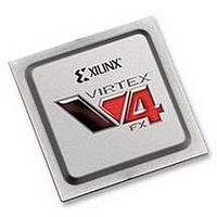
XC4VFX60-10FFG1152C Xilinx Inc, XC4VFX60-10FFG1152C Datasheet - Page 150

XC4VFX60-10FFG1152C
Manufacturer Part Number
XC4VFX60-10FFG1152C
Description
IC FPGA VIRTEX-4 FX 60K 1152FBGA
Manufacturer
Xilinx Inc
Series
Virtex™-4r
Datasheets
1.XC4VFX12-10FFG668C.pdf
(58 pages)
2.XC4VFX12-10FFG668C.pdf
(9 pages)
3.XC4VFX12-10FFG668C.pdf
(406 pages)
Specifications of XC4VFX60-10FFG1152C
Total Ram Bits
4276224
Number Of Logic Elements/cells
56880
Number Of Labs/clbs
6320
Number Of I /o
576
Voltage - Supply
1.14 V ~ 1.26 V
Mounting Type
Surface Mount
Operating Temperature
0°C ~ 85°C
Package / Case
1152-BBGA, FCBGA
No. Of Logic Blocks
6656
No. Of Macrocells
56880
Family Type
Virtex-4
No. Of Speed Grades
10
No. Of I/o's
576
Clock Management
DCM
Core Supply
RoHS Compliant
Package
1152FCBGA
Family Name
Virtex®-4
Device Logic Units
56880
Typical Operating Supply Voltage
1.2 V
Maximum Number Of User I/os
576
Ram Bits
4276224
Lead Free Status / RoHS Status
Lead free / RoHS Compliant
For Use With
HW-V4-ML410-UNI-G - EVALUATION PLATFORM VIRTEX-4
Number Of Gates
-
Lead Free Status / RoHS Status
Lead free / RoHS Compliant
Available stocks
Company
Part Number
Manufacturer
Quantity
Price
Company:
Part Number:
XC4VFX60-10FFG1152C
Manufacturer:
XilinxInc
Quantity:
3 000
Company:
Part Number:
XC4VFX60-10FFG1152C
Manufacturer:
Xilinx Inc
Quantity:
10 000
- XC4VFX12-10FFG668C PDF datasheet
- XC4VFX12-10FFG668C PDF datasheet #2
- XC4VFX12-10FFG668C PDF datasheet #3
- Current page: 150 of 406
- Download datasheet (6Mb)
Chapter 4: Block RAM
FIFO Port Descriptions
150
Table 4-10
Table 4-10: FIFO I/O Port Names and Descriptions
DI
DIP
WREN
WRCLK
RDEN
RDCLK
RESET
DO
DOP
FULL
ALMOSTFULL
EMPTY
ALMOSTEMPTY
RDCOUNT
WRCOUNT
WRERR
RDERR
Port Name
lists the FIFO I/O port names and descriptions.
Direction
Output
Output
Output
Output
Output
Output
Output
Output
Output
Output
Input
Input
Input
Input
Input
Input
Input
www.xilinx.com
Data input.
Parity-bit input.
Write enable. When WREN = 1, data will be written to
memory. When WREN = 0, write is disabled.
Clock for write domain operation.
Read enable. When RDEN = 1, data will be read to output
register. When RDEN = 0, read is disabled.
Clock for read domain operation.
Asynchronous reset of all FIFO functions, flags, and
pointers.
Data output, synchronous to RDCLK.
Parity-bit output, synchronous to RDCLK.
All entries in FIFO memory are filled. No additional write
enable is performed. Synchronous to WRCLK.
Almost all entries in FIFO memory have been filled.
Synchronous to WRCLK. The offset for this flag is user
configurable.
FIFO is empty. No additional read can be performed.
Synchronous to RDCLK.
Almost all valid entries in FIFO have been read.
Synchronous with RDCLK. The offset for this flag is user
configurable.
The FIFO data read pointer. It is synchronous with RDCLK.
The value will wrap around if the maximum read pointer
value has been reached.
The FIFO data write pointer. It is synchronous with
WRCLK. The value will wrap around if the maximum write
pointer value has been reached.
When the FIFO is full, any additional write operation
generates an error flag. Synchronous with WRCLK.
When the FIFO is empty, any additional read operation
generates an error flag. Synchronous with RDCLK.
Description
UG070 (v2.6) December 1, 2008
Virtex-4 FPGA User Guide
R
Related parts for XC4VFX60-10FFG1152C
Image
Part Number
Description
Manufacturer
Datasheet
Request
R

Part Number:
Description:
IC FPGA VIRTEX-4 FX 60K 672-FBGA
Manufacturer:
Xilinx Inc

Part Number:
Description:
IC FPGA VIRTEX-4 FX 60K 672-FBGA
Manufacturer:
Xilinx Inc
Datasheet:

Part Number:
Description:
IC FPGA VIRTEX-4 FX 60K 672-FBGA
Manufacturer:
Xilinx Inc
Datasheet:

Part Number:
Description:
IC FPGA VIRTEX-4 FX 60K 1152FBGA
Manufacturer:
Xilinx Inc
Datasheet:

Part Number:
Description:
IC FPGA VIRTEX-4 FX 60K 1152FBGA
Manufacturer:
Xilinx Inc
Datasheet:

Part Number:
Description:
IC FPGA VIRTEX-4FX 1152FFBGA
Manufacturer:
Xilinx Inc
Datasheet:

Part Number:
Description:
IC FPGA VIRTEX-4FX 1152FFBGA
Manufacturer:
Xilinx Inc
Datasheet:

Part Number:
Description:
FPGA Virtex®-4 Family 56880 Cells 90nm (CMOS) Technology 1.2V 672-Pin FCBGA
Manufacturer:
Xilinx Inc
Datasheet:

Part Number:
Description:
IC FPGA VIRTEX-4 FX 60K 672-FBGA
Manufacturer:
Xilinx Inc
Datasheet:

Part Number:
Description:
IC FPGA VIRTEX-4 FX 60K 672-FBGA
Manufacturer:
Xilinx Inc
Datasheet:

Part Number:
Description:
IC FPGA VIRTEX-4 FX 60K 1152FBGA
Manufacturer:
Xilinx Inc
Datasheet:

Part Number:
Description:
FPGA Virtex®-4 Family 56880 Cells 90nm (CMOS) Technology 1.2V 672-Pin FCBGA
Manufacturer:
Xilinx Inc
Datasheet:

Part Number:
Description:
IC CPLD .8K 36MCELL 44-VQFP
Manufacturer:
Xilinx Inc
Datasheet:

Part Number:
Description:
IC CPLD 72MCRCELL 10NS 44VQFP
Manufacturer:
Xilinx Inc
Datasheet:


