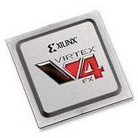
XC4VFX60-10FFG1152C Xilinx Inc, XC4VFX60-10FFG1152C Datasheet - Page 129

XC4VFX60-10FFG1152C
Manufacturer Part Number
XC4VFX60-10FFG1152C
Description
IC FPGA VIRTEX-4 FX 60K 1152FBGA
Manufacturer
Xilinx Inc
Series
Virtex™-4r
Datasheets
1.XC4VFX12-10FFG668C.pdf
(58 pages)
2.XC4VFX12-10FFG668C.pdf
(9 pages)
3.XC4VFX12-10FFG668C.pdf
(406 pages)
Specifications of XC4VFX60-10FFG1152C
Total Ram Bits
4276224
Number Of Logic Elements/cells
56880
Number Of Labs/clbs
6320
Number Of I /o
576
Voltage - Supply
1.14 V ~ 1.26 V
Mounting Type
Surface Mount
Operating Temperature
0°C ~ 85°C
Package / Case
1152-BBGA, FCBGA
No. Of Logic Blocks
6656
No. Of Macrocells
56880
Family Type
Virtex-4
No. Of Speed Grades
10
No. Of I/o's
576
Clock Management
DCM
Core Supply
RoHS Compliant
Package
1152FCBGA
Family Name
Virtex®-4
Device Logic Units
56880
Typical Operating Supply Voltage
1.2 V
Maximum Number Of User I/os
576
Ram Bits
4276224
Lead Free Status / RoHS Status
Lead free / RoHS Compliant
For Use With
HW-V4-ML410-UNI-G - EVALUATION PLATFORM VIRTEX-4
Number Of Gates
-
Lead Free Status / RoHS Status
Lead free / RoHS Compliant
Available stocks
Company
Part Number
Manufacturer
Quantity
Price
Company:
Part Number:
XC4VFX60-10FFG1152C
Manufacturer:
XilinxInc
Quantity:
3 000
Company:
Part Number:
XC4VFX60-10FFG1152C
Manufacturer:
Xilinx Inc
Quantity:
10 000
- XC4VFX12-10FFG668C PDF datasheet
- XC4VFX12-10FFG668C PDF datasheet #2
- XC4VFX12-10FFG668C PDF datasheet #3
- Current page: 129 of 406
- Download datasheet (6Mb)
Virtex-4 FPGA User Guide
UG070 (v2.6) December 1, 2008
Optional Output Register On/Off Switch - DO[A|B]_REG
Clock Inversion at Output Register Switch - INVERT_CLK_DO[A|B]_REG
Extended Mode Address Determinant - RAM_EXTENSION_[A|B]
Read Width - READ_WIDTH_[A|B]
Write Width - WRITE_WIDTH_[A|B]
Write Mode - WRITE_MODE_[A|B]
Block RAM Location Constraints
R
Table 4-5: Port Width Values
This attribute sets the number of pipeline register at A/B output of RAMB16. The valid
values are 0 (default) or 1.
When set to TRUE, the clock input to the pipeline register at A/B output of RAMB16 is
inverted. The default value is FALSE.
This attribute determines whether the block RAM of interest has its A/B port as
UPPER/LOWER address when using the cascade mode. Refer to the
RAM”
NONE.
This attribute determines the A/B read port width of the block RAM. The valid values are:
0 (default), 1, 2, 4, 9, 18, and 36.
This attribute determines the A/B write port width of the block RAM. The valid values are:
0 (default), 1, 2, 4, 9, 18, and 36.
This attribute determines the write mode of the A/B input ports. The possible values are
WRITE_FIRST (default), READ_FIRST, and NO_CHANGE. Additional information on the
write modes is in the
Block RAM instances can have LOC properties attached to them to constrain placement.
Block RAM placement locations differ from the convention used for naming CLB locations,
allowing LOC properties to transfer easily from array to array.
Port Data Width
section. When the block RAM is not used in cascade mode, the default value is
18
36
1
2
4
9
“Operating Modes”
www.xilinx.com
DOP Bus
<1:0>
<3:0>
NA
NA
NA
<0>
section.
DO Bus
<15:0>
<31:0>
<1:0>
<3:0>
<7:0>
<0>
Block RAM Attributes
“Cascadable Block
INIT / SRVAL
(4 + 32) = 36
(2 + 16) = 18
(1 + 8) = 9
1
2
4
129
Related parts for XC4VFX60-10FFG1152C
Image
Part Number
Description
Manufacturer
Datasheet
Request
R

Part Number:
Description:
IC FPGA VIRTEX-4 FX 60K 672-FBGA
Manufacturer:
Xilinx Inc

Part Number:
Description:
IC FPGA VIRTEX-4 FX 60K 672-FBGA
Manufacturer:
Xilinx Inc
Datasheet:

Part Number:
Description:
IC FPGA VIRTEX-4 FX 60K 672-FBGA
Manufacturer:
Xilinx Inc
Datasheet:

Part Number:
Description:
IC FPGA VIRTEX-4 FX 60K 1152FBGA
Manufacturer:
Xilinx Inc
Datasheet:

Part Number:
Description:
IC FPGA VIRTEX-4 FX 60K 1152FBGA
Manufacturer:
Xilinx Inc
Datasheet:

Part Number:
Description:
IC FPGA VIRTEX-4FX 1152FFBGA
Manufacturer:
Xilinx Inc
Datasheet:

Part Number:
Description:
IC FPGA VIRTEX-4FX 1152FFBGA
Manufacturer:
Xilinx Inc
Datasheet:

Part Number:
Description:
FPGA Virtex®-4 Family 56880 Cells 90nm (CMOS) Technology 1.2V 672-Pin FCBGA
Manufacturer:
Xilinx Inc
Datasheet:

Part Number:
Description:
IC FPGA VIRTEX-4 FX 60K 672-FBGA
Manufacturer:
Xilinx Inc
Datasheet:

Part Number:
Description:
IC FPGA VIRTEX-4 FX 60K 672-FBGA
Manufacturer:
Xilinx Inc
Datasheet:

Part Number:
Description:
IC FPGA VIRTEX-4 FX 60K 1152FBGA
Manufacturer:
Xilinx Inc
Datasheet:

Part Number:
Description:
FPGA Virtex®-4 Family 56880 Cells 90nm (CMOS) Technology 1.2V 672-Pin FCBGA
Manufacturer:
Xilinx Inc
Datasheet:

Part Number:
Description:
IC CPLD .8K 36MCELL 44-VQFP
Manufacturer:
Xilinx Inc
Datasheet:

Part Number:
Description:
IC CPLD 72MCRCELL 10NS 44VQFP
Manufacturer:
Xilinx Inc
Datasheet:


